Semiconductor device

a semiconductor and storage device technology, applied in the direction of semiconductor devices, electrical devices, transistors, etc., can solve the problems of loss of trapped charges, and achieve the effect of restoring crystal defects and wishing to further enhance memory characteristics

Inactive Publication Date: 2007-05-15
SEIKO EPSON CORP
View PDF2 Cites 9 Cited by
  • Summary
  • Abstract
  • Description
  • Claims
  • Application Information

AI Technical Summary

Benefits of technology

[0006]In the above semiconductor storage device, the thermal oxide film 132 serves to recover damage due to etching when patterning the gate electrode, and restore crystal defect. This thermal oxide film 132, however, is not formed on a side surface of the ONO film 120. Specifically, etching damage and crystal defect caused on the end surface of the ONO film 120 are not recovered. This contributes to loss of trapped charges such that there is the case where electrons are not trapped well. Thus, a memory characteristic is desired to be further enhanced.
[0009]In the semiconductor storage device according to an aspect of the present invention, charges are trapped into the charge trapping layer in the vicinity of the end surface of the gate electrode, and thereby writing is implemented. It therefore is preferable that there is no etching damage and crystal fault around the position where charges are trapped. According to the semiconductor storage device of an aspect of the invention, the end surface of the stacked body is positioned outside the end surface of the gate electrode such that the end surface of the charge trapping layer is provided at the position distant from a position where charges are trapped when writing. Accordingly, a MONOS type semiconductor storage device with high reliability that can reduce loss of charges, even in the case where damage is caused in the end surface of the charge trapping layer, can be provided.
[0017]According to a method of manufacturing a semiconductor storage device of an aspect of the invention, the stacked body is formed by etching the stacked film while utilizing the side wall insulating layer as a mask. The end surface of the charge trapping layer therefore is provided at a position distant by a given length from the side surface of the gate electrode. In the semiconductor storage device according to an aspect of the present invention, charges are trapped into the charge trapping layer around the side surface of the gate electrode, and thereby writing is implemented. It therefore is preferable that there is no damage, such as crystal defect in the charge trapping layer in the vicinity of the position where charges are trapped. According to a method of manufacturing a semiconductor storage device of an aspect of the invention, the end surface of the charge trapping layer can be formed at a position distant from the position where charges are trapped when writing. Accordingly, a non-volatile semiconductor storage device with high reliability that can reduce loss of charges even in the case where damage is caused in the end surface of the charge trapping layer, can be manufactured.
[0019]According to a method of manufacturing a semiconductor storage device of an aspect of the invention, the stacked body is formed in a manner of having a pattern different from that of the gate electrode. Specifically, the end surface of the stacked body is positioned with a given distance from the position of the side surface of the gate electrode. In the semiconductor storage device according to an aspect of the invention, charges are trapped into the charge trapping layer in the vicinity of the side surface of the gate electrode, and thereby writing is implemented. It therefore is preferable that there is no damage, such as crystal defect in the charge trapping layer in the vicinity of the position where charges are trapped. According to a method of manufacturing a semiconductor storage device of an aspect of the invention, the end surface of the charge trapping layer can be formed at a position distant from the position where charges are trapped when writing. Accordingly, a non-volatile semiconductor storage device with high reliability that can reduce loss of charges even in the case where damage is caused in the end surface of the charge trapping layer, can be manufactured.

Problems solved by technology

This contributes to loss of trapped charges such that there is the case where electrons are not trapped well.

Method used


Image

  • Semiconductor device
  • Semiconductor device
  • Semiconductor device

Examples


first exemplary embodiment

3.1 First Exemplary Embodiment

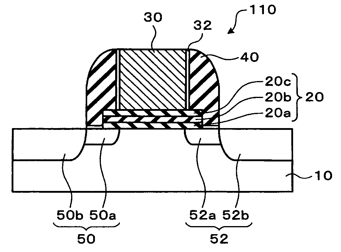
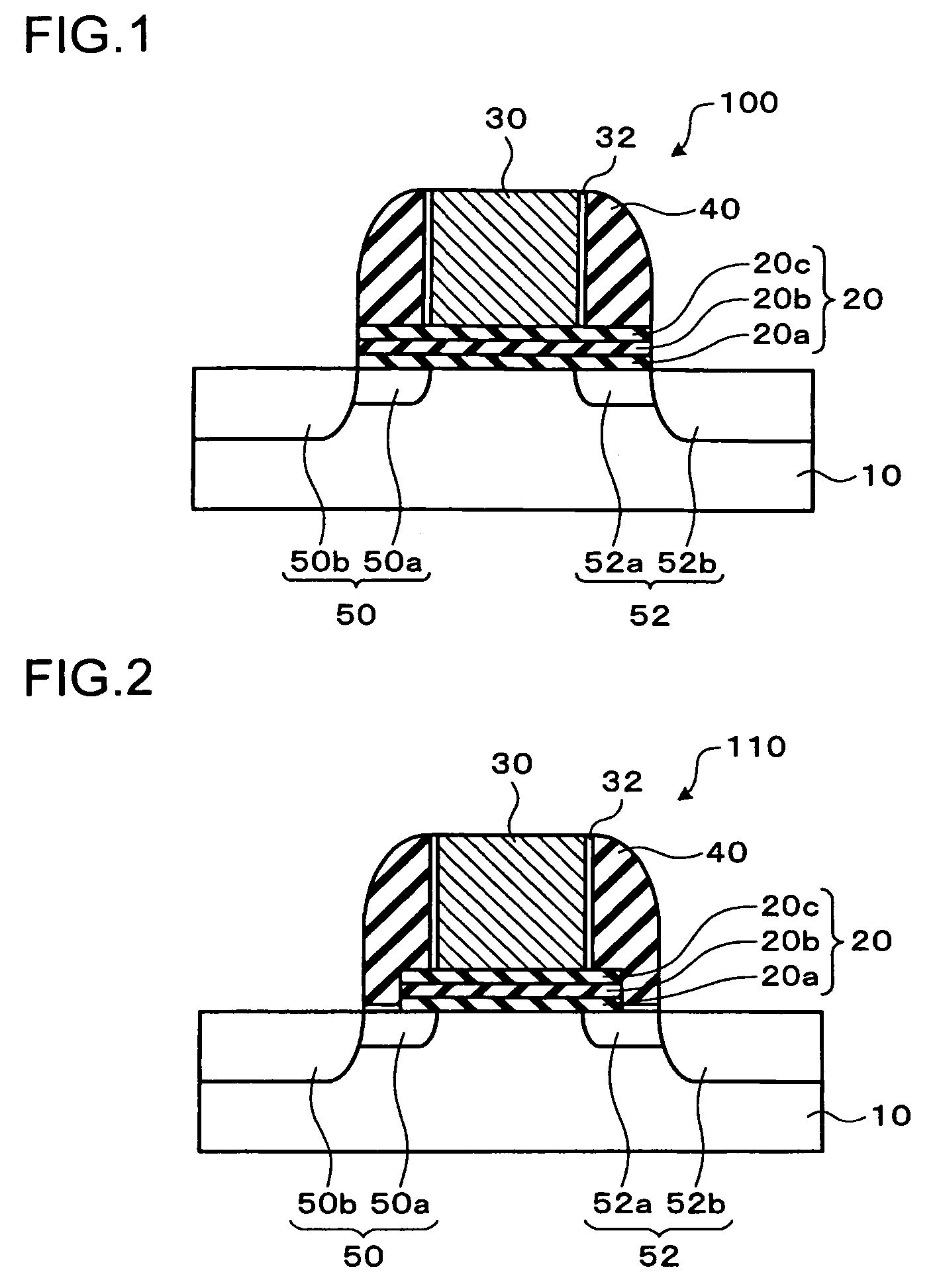
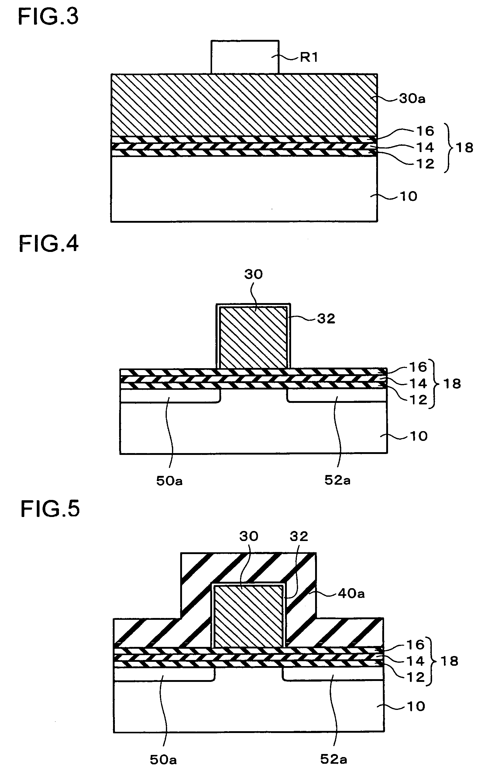
[0039]A method of manufacturing the semiconductor storage device shown in FIG. 1 will be described with reference to FIGS. 3 through 5. Each sectional view corresponds to the sectional view shown in FIG. 1. In FIGS. 3 through 5, the same numerals are given to the elements which are substantially the same as those shown in FIG. 1, and the overlapping description will be omitted.

[0040](1) First, a stacked film 18 including a first insulating layer, a charge trapping layer, and a second insulating layer is formed on a surface of the semiconductor layer 10 (refer to FIG. 3). As the stacked film 18, an ONO film is formed.

[0041]In the forming of the stacked film 18, first, a first insulating layer 12 composed of oxide silicon is formed on a surface of the semiconductor substrate 10, which is a semiconductor layer, by a thermal oxidization method. A CVD method, instead of a thermal oxidization method, may be used for the formation of the first insulating layer...

second exemplary embodiment

3.2 Second Exemplary Embodiment

[0051]A method of manufacturing a semiconductor storage device according to a second exemplary embodiment will be described with reference to FIGS. 6 through 8. With respect to processes that can be implemented in the same way as the first exemplary embodiment, detailed description will be omitted.

[0052](1) First, as shown in FIG. 4, the gate electrode 30 having a given pattern is formed on the stacked film 18 where the first insulating layer 12, the charge trapping layer 14, and the second insulating layer 16 are stacked, to each other as with the above exemplary embodiment.

[0053](2) Then, as shown in FIG. 6, a mask layer is formed in a manner of covering part of the stacked film 18 formed of the first insulating layer 12, the charge trapping layer 14 and the second insulating layer 16, and the gate electrode 30. As the mask layer, a resist layer R2 is formed, for example, as shown in FIG. 6. Then, the stacked film 18 is etched utilizing the resist la...


PUM


Abstract

A semiconductor storage device showing a good memory characteristic, and a manufacturing method thereof, includes a semiconductor layer, a stacked body including a first insulating layer, a charge trapping layer, and a second insulating layer that are provided above the semiconductor layer, a gate electrode provided above the stacked body, a side wall insulating layer provided at the side of the gate electrode, and impurity regions and provided in the semiconductor layer. The end surface of the stacked body is positioned outside the end surface of the gate electrode.

Description

BACKGROUND OF THE INVENTION[0001]1. Field of Invention[0002]The present invention relates to an insulating-film trapping type non-volatile semiconductor storage device (hereinafter “MONOS”) and a manufacturing method thereof.[0003]2. Description of Related Art[0004]As a semiconductor storage device capable of electrically writing and erasing, there has been a non-volatile semiconductor storage device, which can retain stored date even when power for a memory is eliminated. As such a semiconductor storage device, there is a MONOS type semiconductor storage device.[0005]A MONOS type semiconductor storage device 1000 according to a related art example is shown in FIG. 9. In the semiconductor storage device 1000, a gate electrode 130 is formed above a semiconductor substrate 110 with an ONO film 120 therebetween. A thermal oxide film 132 is formed on a side surface of the gate electrode 130, and a surface of the semiconductor substrate 110 where a side wall insulating layer 140 is forme...

Claims


Application Information

Patent Timeline
Patent Type & Authority Patents(United States)
IPC IPC(8): H01L29/788H01L21/8247H01L21/28H01L21/336H01L27/10H01L27/115H01L29/792
CPCH01L21/28282H01L29/66833H01L29/792H01L29/40117
Inventor MORI, KATSUMI
Owner SEIKO EPSON CORP
Why Eureka
Try Eureka