Growth of reduced dislocation density non-polar gallium nitride by hydride vapor phase epitaxy

a gallium nitride and vapor phase technology, applied in the direction of crystal growth process, polycrystalline material growth, chemically reactive gas, etc., can solve the problem of further charge separation within quantum heterostructures, electron segregation and hole segregation in each layer, and the inability to simply cut a crystal, etc. problem, to achieve the effect of reducing the densities of threading

Inactive Publication Date: 2007-05-22
JAPAN SCI & TECH CORP +1
View PDF33 Cites 105 Cited by
  • Summary
  • Abstract
  • Description
  • Claims
  • Application Information

AI Technical Summary

Benefits of technology

[0020]The present invention discloses a method of performing a lateral epitaxial overgrowth of a planar, non-polar, a-plane GaN film, comprising: (a) patterning a mask deposited on a substrate; and (b) performing a lateral epitaxial overgrowth of the GaN film off the substrate using hydride vapor phase epitaxy, wherein the GaN film nucleates only on portions of the substrate not covered by the patterned mask, the GaN film grows vertically through openings in the patterned mask, and the GaN film then spreads laterally above the patterned mask and across the substrate's surface. The lateral epitaxial overgrowth reduces threading dislocation densities in the GaN film.

Problems solved by technology

A negative consequence of this growth direction is that each layer material will suffer from segregation of electrons and holes to opposite faces of the layers due to the spontaneous polarization of the crystal.
Furthermore, strain at the interfaces between adjacent layers gives rise to piezoelectric polarization, causing further charge separation within quantum heterostructures.
Bulk crystals of GaN are not available so it is not possible to simply cut a crystal to present a surface for subsequent device regrowth.
While this work represents an enabling technology for the growth of non-polar GaN devices, the relatively high defect density in the directly-grown a-GaN films reduces the efficiency of subsequently grown devices compared to what could be achieved by homoepitaxial growth on a perfect substrate.
The two predominant types of extended defects of concern are threading dislocations and stacking faults.
However, HVPE-based LEO of a-plane GaN has not previously been accomplished.

Method used


Image

  • Growth of reduced dislocation density non-polar gallium nitride by hydride vapor phase epitaxy
  • Growth of reduced dislocation density non-polar gallium nitride by hydride vapor phase epitaxy
  • Growth of reduced dislocation density non-polar gallium nitride by hydride vapor phase epitaxy

Examples


Embodiment Construction

[0032]In the following description of the preferred embodiment, reference is made to the accompanying drawings which form a part hereof, and in which is shown by way of illustration a specific embodiment in which the invention may be practiced. It is to be understood that other embodiments may be utilized and structural changes may be made without departing from the scope of the present invention.

[0033]Overview

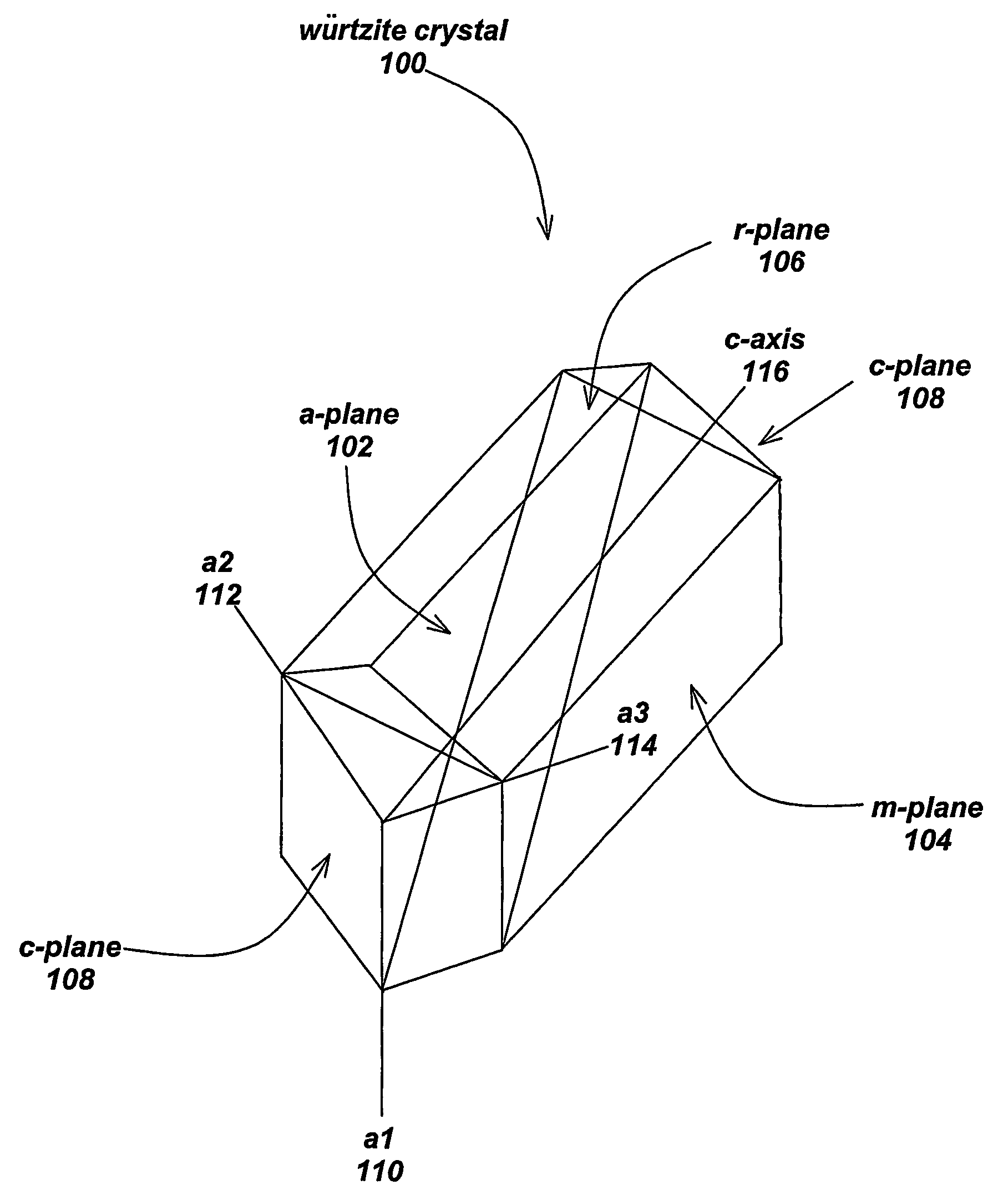
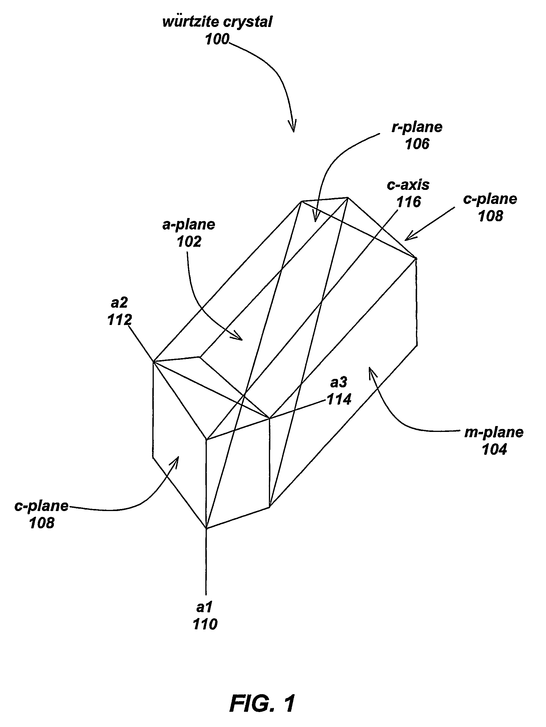
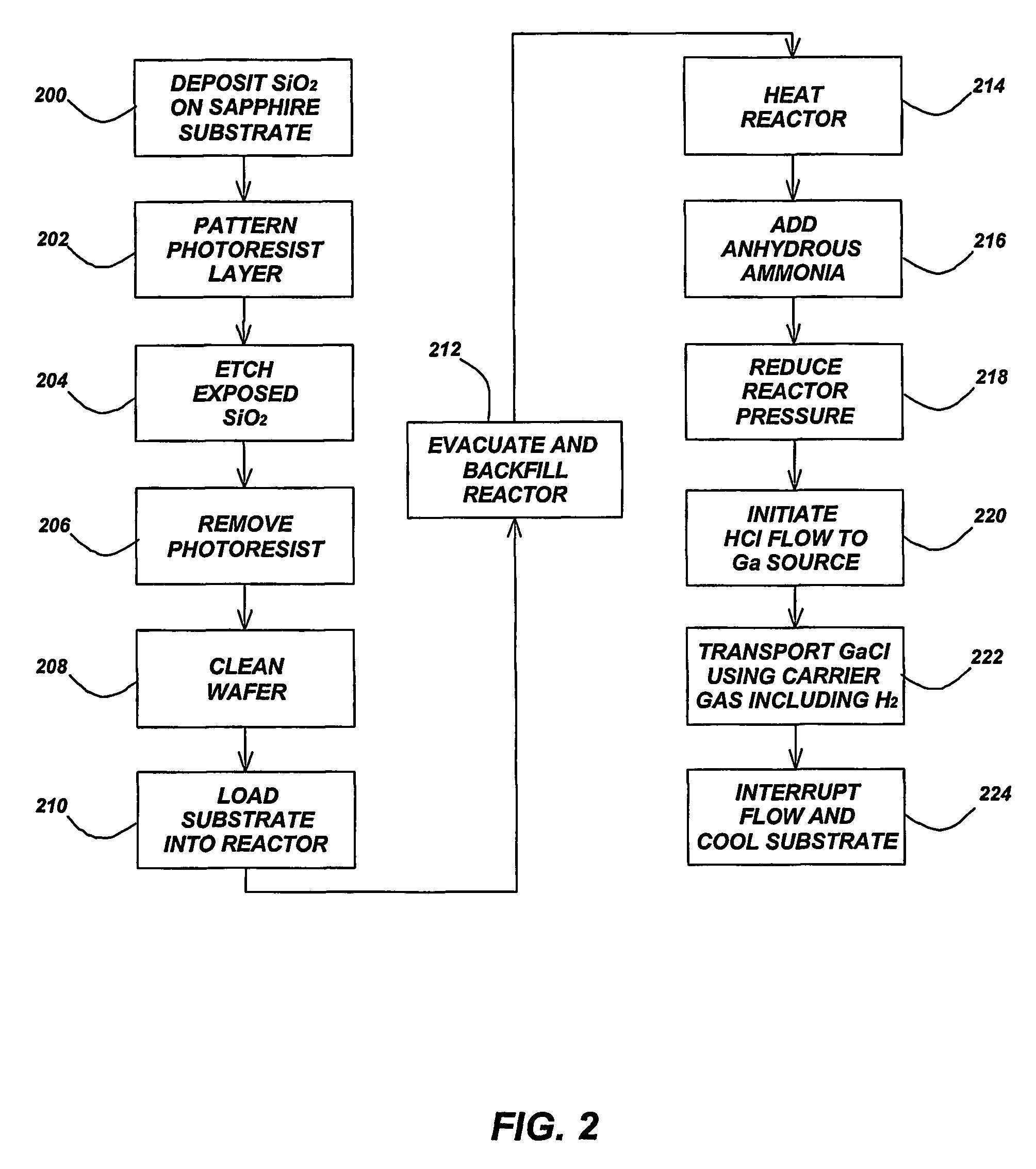
[0034]The present invention reduces threading dislocation densities in HVPE-grown non-polar, a-plane GaN films using LEO. By utilizing reduced growth pressures and a carrier gas containing a fraction of hydrogen, lateral growth of a non-polar GaN film directly off a foreign substrate can be achieved. A patterned mask is applied to the substrate through one of a variety of means. The substrate is then loaded into a HVPE reactor and the a-GaN film grows only from the regions of exposed substrate material and spreads laterally above the mask and across the substrate surface.

[0035...


PUM

PropertyMeasurementUnit
pressureaaaaaaaaaa
pressureaaaaaaaaaa
thickaaaaaaaaaa

Abstract

Lateral epitaxial overgrowth (LEO) of non-polar a-plane gallium nitride (GaN) films by hydride vapor phase epitaxy (HVPE) results in significantly reduced defect density.

Description

CROSS-REFERENCE TO RELATED APPLICATIONS[0001]This application claims priority to the following co-pending and commonly-assigned U.S. Provisional Patent Applications:[0002]Ser. No. 60 / 433,843, entitled “GROWTH OF REDUCED DISLOCATION DENSITY NON-POLAR GALLIUM NITRIDE BY HYDRIDE VAPOR PHASE EPITAXY,” filed on Dec. 16, 2002, by Benjamin A. Haskell, Michael D. Craven, Paul T. Fini, Steven P. DenBaars, James S. Speck, and Shuji Nakamura, and[0003]Ser. No. 60 / 433,844, entitled “TECHNIQUE FOR THE GROWTH OF PLANAR, NON-POLAR A-PLANE GALLIUM NITRIDE BY HYDRIDE VAPOR PHASE EPITAXY,” filed on Dec. 16, 2002, by Benjamin A. Haskell, Paul T. Fini, Shigemasa Matsuda, Michael D. Craven, Steven P. DenBaars, James S. Speck, and Shuji Nakamura,[0004]both of which applications are incorporated by reference herein.[0005]This application is related to co-pending and commonly-assigned International Application No. PCT / US03 / 21916, entitled “GROWTH OF PLANAR, NON-POLAR A-PLANE GALLIUM NITRIDE BY HYDRIDE VAPO...

Claims


Application Information

Patent Timeline
Patent Type & Authority Patents(United States)
IPC IPC(8): H01L21/20C30B25/02H01L21/205
CPCC30B25/02C30B29/403C30B29/406H01L21/0242H01L21/02433H01L21/02647H01L21/0254H01L21/02609H01L21/0262H01L21/02639H01L21/02458
Inventor HASKELL, BENJAMIN ACRAVEN, MICHAEL D.FINI, PAUL T.DENBAARS, STEVEN P.SPECK, JAMES S.NAKAMURA, SHUJI
Owner JAPAN SCI & TECH CORP
Why Eureka
Try Eureka