On-chip termination with calibrated driver strength

a technology of driver strength and on-chip termination, which is applied in the direction of pulse generator, pulse technique, digital transmission, etc., can solve the problems of degrading the overall signal integrity, consuming a substantial amount of board space, and a large amount of external termination resistors

Inactive Publication Date: 2007-05-22
ALTERA CORP
View PDF73 Cites 69 Cited by
  • Summary
  • Abstract
  • Description
  • Claims
  • Application Information

AI Technical Summary

Problems solved by technology

When transmitting signals over distances that are appreciable with respect to the signal period, mismatches between the impedance of the transmission line and that of the receiver cause signal reflection.
The reflected signal interferes with the transmitted signal and causes distortion and degrades the overall signal integrity.
For many of today's high speed integrated circuits, and particularly those that have large I / O pin counts, external termination poses a number of problems.
Numerous external termination resistors can consume a substantial amount of board space.
The use of external components for termination purposes can be cumbersome and costly, especially in the case of an integrated circuit with numerous I / O pins.

Method used


Image

  • On-chip termination with calibrated driver strength
  • On-chip termination with calibrated driver strength
  • On-chip termination with calibrated driver strength

Examples


Embodiment Construction

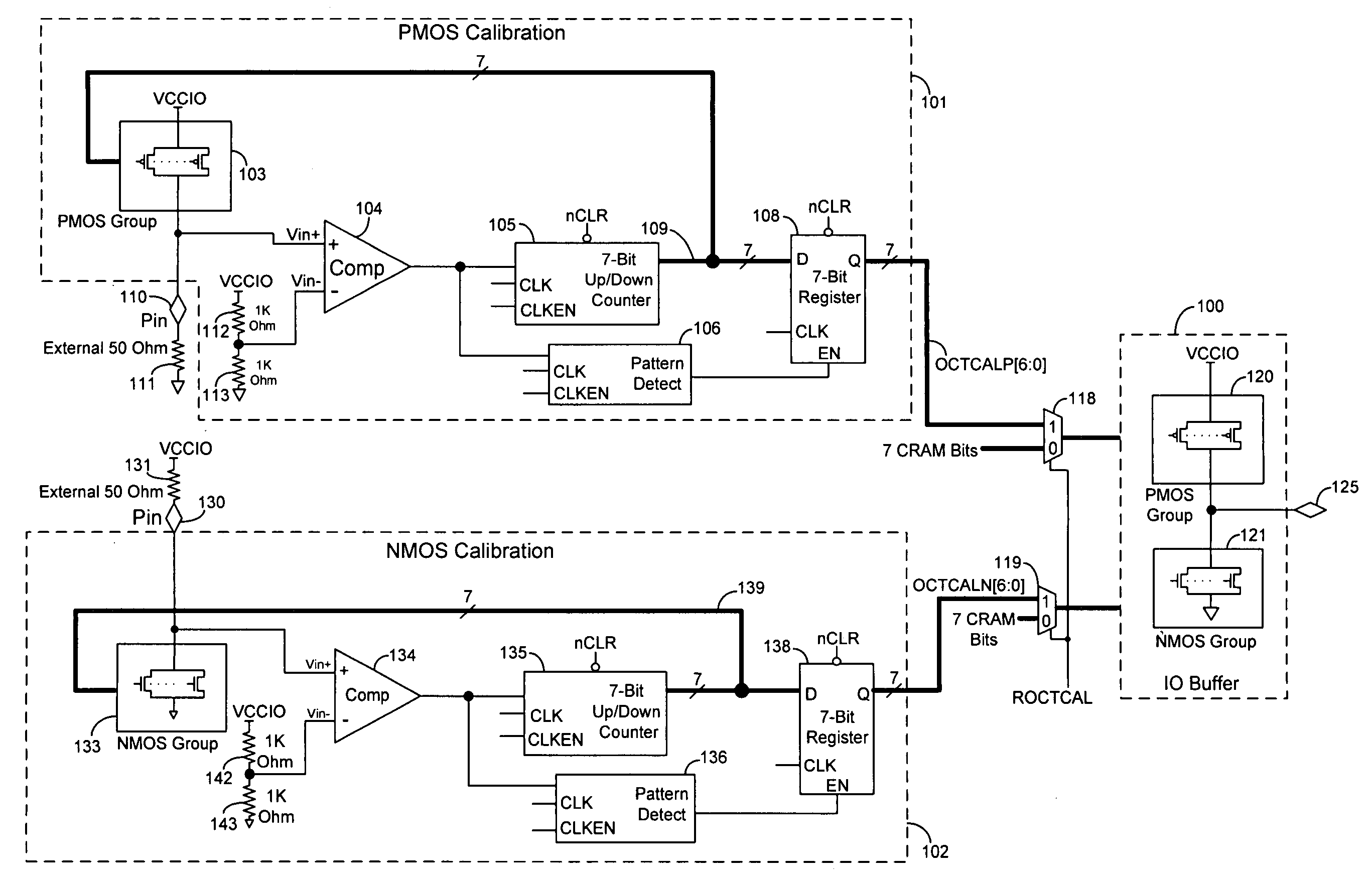
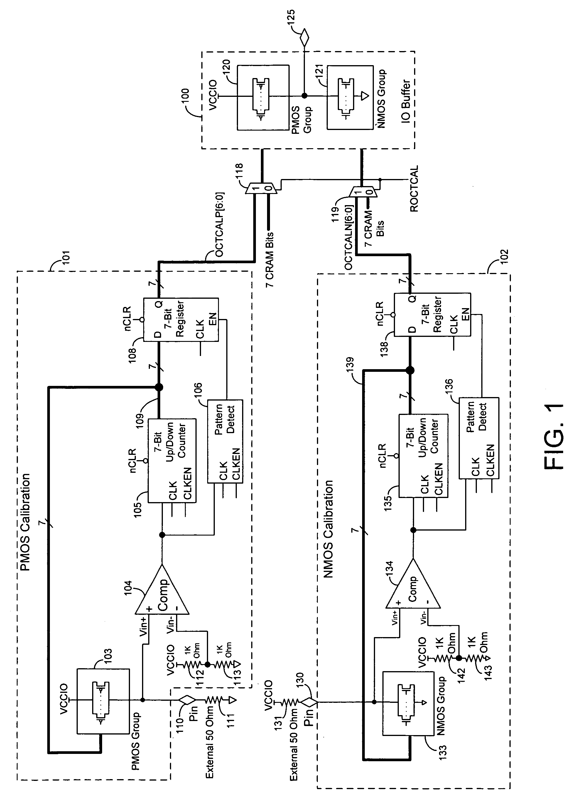
[0015]FIG. 1 illustrates a PMOS calibration circuit 101 and an NMOS calibration circuit 102 according to embodiments of the present invention. PMOS calibration circuit 101 controls the series termination resistance of pull-up PMOS transistors 120 in input / output (IO) buffer 100. NMOS calibration circuit 102 controls the series termination resistance of pull-down NMOS transistors 121 in IO buffer 100. Transistor groups 120 and 121 drive output signals to IO pin 125.

[0016]The transistors in groups 120 and 121 are binary-weighted, parallel-connected transistors. For example, transistor groups 120 and 121 can each have 7 transistors with channel width-to-length (W / L) ratios of 1×, 2×, 4×, 8×, 16×, 32×, and 64×. The transistors in groups 120 and 121 are controlled by configurable RAM (CRAM) bits or by calibration signals from circuits 101 and 102. The total drive current strength provided to pin 125 equals the sum of the transistor currents in driver 100. The impedance of driver 100 is i...


PUM


Abstract

Techniques are provided for controlling an on-chip termination resistance in an input or output (IO) buffer using calibration circuits. Each calibration circuit monitors the voltage between an external resistor and a group of on-chip transistors. When the effective resistance of the group of transistors matches the external resistance, the calibration circuit causes the effective resistance of drive transistors in the IO buffer to match the effective resistance of the group of on-chip transistors.

Description

CROSS-REFERENCES TO RELATED APPLICATIONS[0001]This patent application is related to commonly-assigned, co-pending U.S. patent application Ser. No. 11 / 040,343, filed Jan. 20, 2005, by Chang et al., which is incorporated by reference herein.BACKGROUND OF THE INVENTION[0002]The present invention relates to techniques for controlling on-chip termination resistance using calibrated drive strength, and more particularly, to techniques for monitoring an effective resistance of on-chip transistors to control the drive strength provided to an input / output pin to provide on-chip termination impedance matching.[0003]When transmitting signals over distances that are appreciable with respect to the signal period, mismatches between the impedance of the transmission line and that of the receiver cause signal reflection. The reflected signal interferes with the transmitted signal and causes distortion and degrades the overall signal integrity. To minimize or eliminate the unwanted reflection, tran...

Claims


Application Information

Patent Timeline
Patent Type & Authority Patents(United States)
IPC IPC(8): H03B1/00
CPCH03K19/0005H04L25/0298
Inventor WANG, XIAOBAOCHANG, TZUNG-CHINSUNG, CHIAKANGNGUYEN, KHAI Q.
Owner ALTERA CORP
Why Eureka
Try Eureka