Radio frequency identification tag and method of making the same

a radio frequency identification and tag technology, applied in the field of wireless communication, can solve the problems of affecting the mass production of suitable tags, affecting the large-scale production of rfid tags, and affecting the maintenance, operation and manufacture of such tags, and achieves the effects of high fidelity, reliable and efficient operation

Active Publication Date: 2007-05-22
TRACKING TECH
View PDF12 Cites 33 Cited by
  • Summary
  • Abstract
  • Description
  • Claims
  • Application Information

AI Technical Summary

Benefits of technology

[0011]Accordingly, the present invention includes an efficient, reliable, and high fidelity RFID tag and a method of making the same. The RFID tag of the present invention includes a substrate, upon which an antenna for receiving and transmitting radio frequency signals may be printed. The RFID tag also includes a die positioning structure disposed on the substrate that is cast and cured specifically for receiving a silicon die of the type typically used in RFID applications. The silicon die is electrically connected to the antenna through at least one bond, which enables the RFID tag to transmit, receive, and possibly update electronic data stored on the silicon die through normal RFID protocols.
[0012]In varying embodiments, the RFID tag of the present invention is operable over a range of frequencies that enable it to be operable over a range of applications and jurisdictions. For example, the antenna may be selected such that it is operable between 400 and 1000 Megahertz. More particularly, for improved operation in the United States, the antenna may be selected to be operable between 915 and 920 Megahertz. For low frequency applications, the selected antenna would be operable between 100 and 150 kilohertz, while for microwave applications the antenna would be operable between 2.4 and 2.5 Gigahertz. Thus, the RFID tag of the present invention is readily adapted to use over a range of frequencies, and thus may be used in across a range of applications, from a variety of consumer products to automotive components and animal identification tags.
[0013]The novel RFID tag of the present invention is the result of an improved method of manufacture in the RFID industry. The method includes a number of acts, including providing a substrate with an antenna printed thereon and a second material. The substrate is generally of a dielectric material and hydrophobic, and should preferably be of low stopping power for electron beam radiation. The second material is curable by electron beam radiation, and is disposed on the substrate through a pressing mechanism that forms the die positioning structure discussed above. Once the die positioning structure is cured and affixed to the substrate, a silicon die is positioned within the die positioning structure and connected to the antenna through at least one bonding point. At this time, a manufacturer may provide a radio signal receivable by the antenna to test the electrical connections of the RFID tag. Once the operability of the RFID tag is confirmed, a protective cap or coating is disposed over the silicon die and the die positioning structure to increase the resiliency and abrasive resistance of the RFID tag.

Problems solved by technology

In spite of the advantages of the passive tag, there are numerous problems encountered with their maintenance, operation, and manufacture.
In particular, given the sheer volume of commerce and the potential market for RFID tags, there are currently severe limitations in the manufacturing process that hinder the mass production of suitable tags.
The process outlined above presents a number of complications that hinder the large-scale production of RFID tags.
First, as the economic demand for RFID tags reaches into the billions of units per year, the 8–10 second UV-curing process effectively limits the supply that manufacturers can theoretically muster.
Secondly, once the die is bonded to the antenna, there is no simple method for removing the die if it fails to perform in the pre-shipment tests.
Consequently, an estimated 20–40% of the RFID tags that fail the tests are irrevocably lost, further limiting the supply and increasing the cost of tags to businesses and consumers.

Method used


Image

  • Radio frequency identification tag and method of making the same
  • Radio frequency identification tag and method of making the same
  • Radio frequency identification tag and method of making the same

Examples


Embodiment Construction

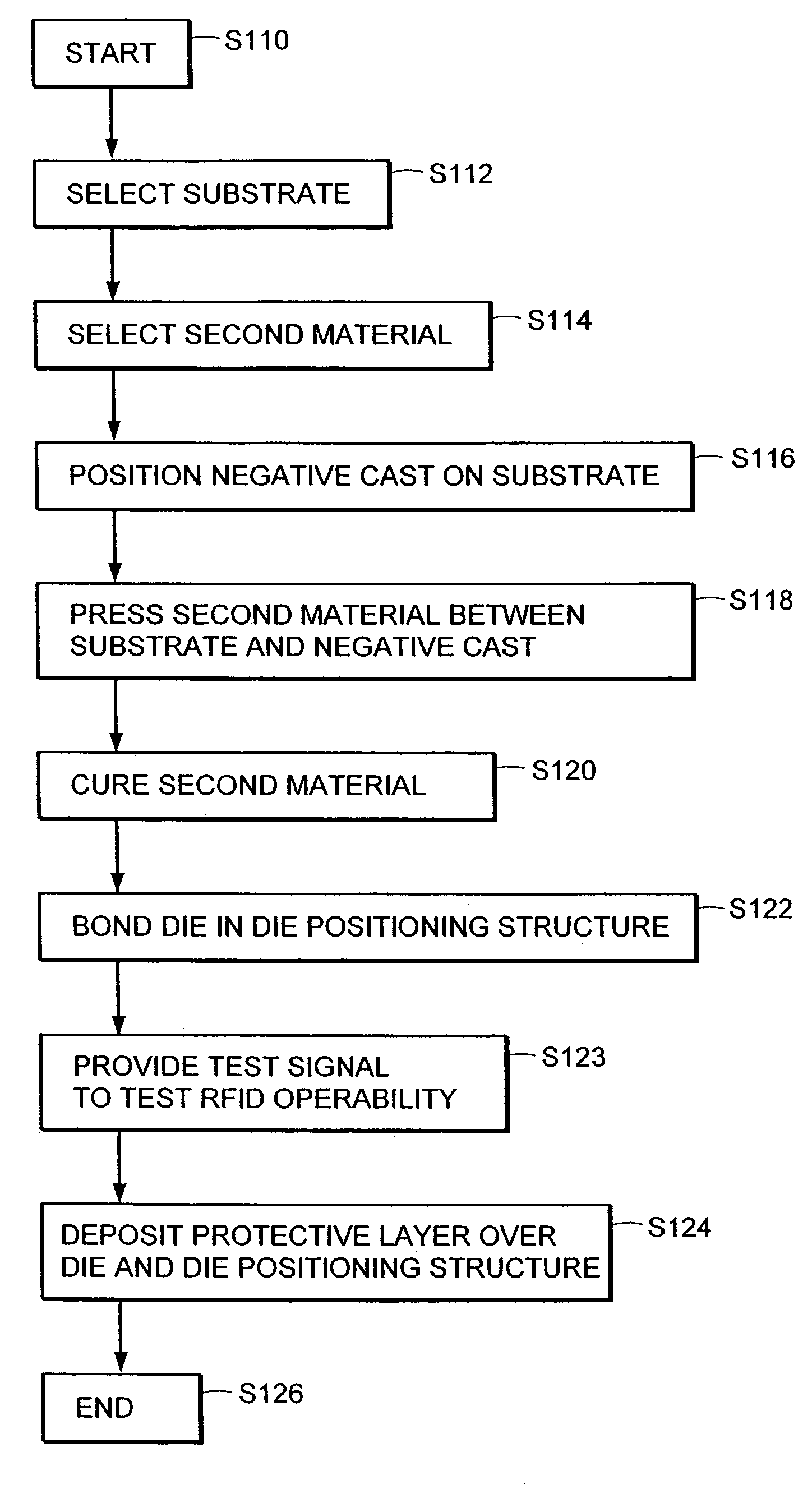
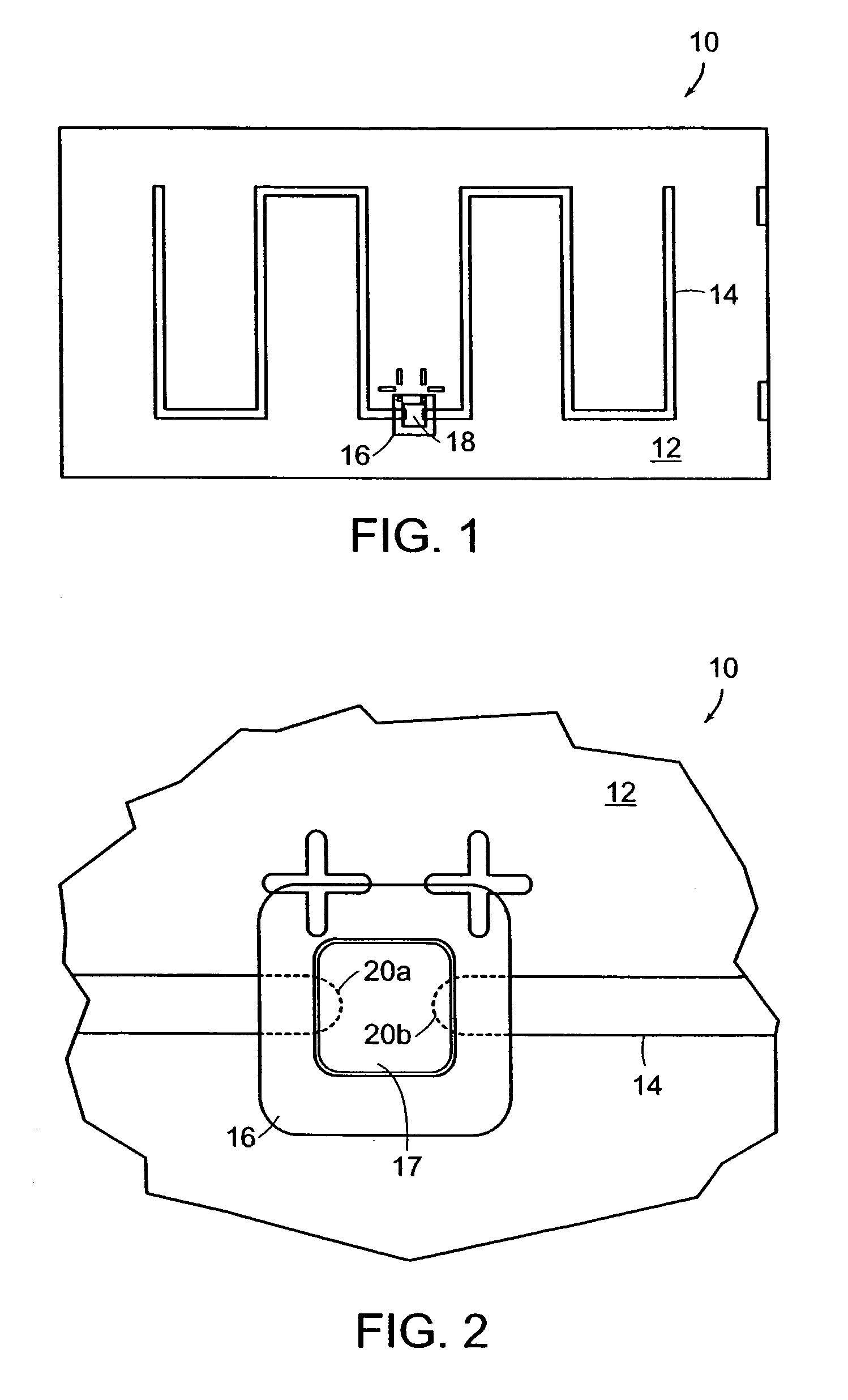
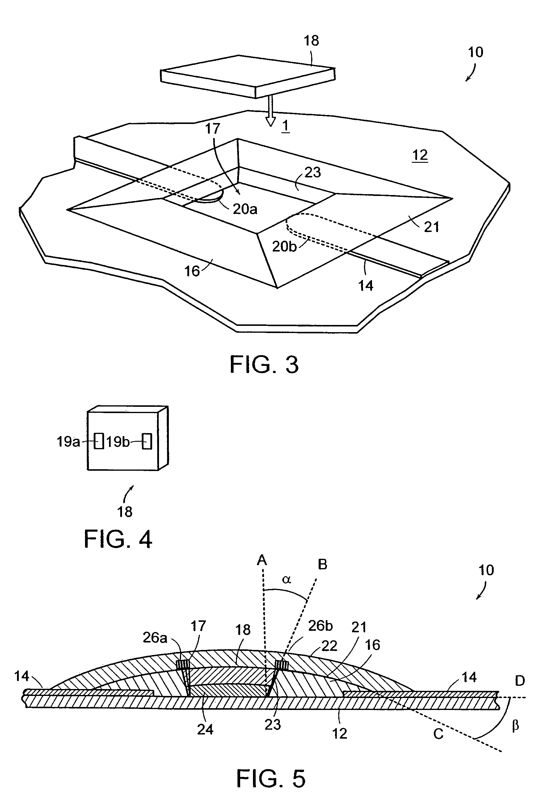
[0026]Two embodiments of the invention to accommodate the silicon die in a normal (bond pads up) and flip chip (bond pads down) orientation are presented here. In accordance with a preferred embodiment of the present invention, FIG. 1 illustrates a plan view of an RFID tag 10. The RFID tag 10 includes a substrate 12 and an antenna 14 that is located upon the substrate 12. The RFID tag 10 further includes a die positioning structure 16 in which a silicon die 18 is disposed.

[0027]The details of the RFID tag 10 are shown in FIG. 2, which is a detailed plan view of the present invention. As shown in FIG. 2, the die positioning structure 16 is disposed on the substrate 12 such that it overlaps the antenna 14. The die positioning structure 16 is disposed such that it substantially overlaps antenna leads 20a, 20b. The die positioning structure 16 defines in part a die positioning cavity 17, which is also located such that it substantially overlaps the antenna leads 20a, 20b in such a manne...


PUM


Abstract

The present invention describes a process for manufacture of RFID tags. The RFID tag of the present invention includes a substrate, an antenna, and a die positioning structure disposed on the substrate that is cast and cured specifically for receiving a silicon die of the type typically used in RFID applications. The substrate is selected from a number of materials, the properties of which render it penetrable by electron beam radiation. The die positioning structure is a second material which is electron beam curable, and which is deposited and cured at high speed on the substrate in a novel fashion in accordance with the present invention in a highly efficient, reproducible and economical manner.

Description

BACKGROUND OF THE INVENTION[0001]1. Field of the Invention[0002]The present invention relates generally to the field of wireless communications, and specifically to the use of radio frequency transmissions to track the movement of commercial goods, as well as other suitable applications.[0003]2. Description of the Related Art[0004]Consumers are familiar with electronic systems for recognizing, tabulating, and indexing the movement of goods through the chain of commerce. Everyday examples include bar codes combined with optical scanners as found in a supermarket. More recently, some products and their containers have been “tagged” with radio frequency identification (RFID) transponders, which in combination with a radio frequency reader and sophisticated computer systems, enable a commercial enterprise to track inventory from a distance. An RFID system includes a tag, a reader, and a computer network connected to the reader for compiling the relevant data.[0005]RFID tags generally co...

Claims


Application Information

Patent Timeline
Patent Type & Authority Patents(United States)
IPC IPC(8): G08B13/14G06K19/06
CPCG06K19/07749G06K19/0775
Inventor CARON, MICHAEL ROGERNABLO, SAMUEL V.FRAZIER, JOHN PAUL
Owner TRACKING TECH
Why Eureka
Try Eureka