
Switch circuit and composite high frequency elements

a high frequency element and switch circuit technology, applied in the field of switch circuits, can solve the problems of further reducing transmission loss, and achieve the effects of reducing the transmission loss of receiving signals, increasing width, and being convenient to us

Active Publication Date: 2007-05-22
HITACHI METALS LTD
View PDF28 Cites 13 Cited by
  • Summary
  • Abstract
  • Description
  • Claims
  • Application Information

AI Technical Summary

Benefits of technology

[0014]Another object of the present invention is to provide a small high-frequency composite part with low transmission loss comprising such switch circuit in a multi-layer substrate.DISCLOSURE OF THE INVENTION
[0026]With the above structure, the impedance of the fifth and sixth ports of the second switch means can be controlled, thereby achieving matching with a receiving circuit connected to each port and thus reducing the transmission loss of a receiving signal.
[0027]When the first inductance element is formed by a transmission line such as a strip line, etc. in a multi-layer substrate formed by laminating ceramic sheets, it is preferable to adjust characteristic impedance by a gap between the transmission line and a ground and the width of the transmission line. To provide the transmission line constituting the first inductance element with characteristic impedance lower than 50Ω, the transmission line preferably has an increased width. A wide transmission line has a small characteristic impedance and a reduced resistance, resulting in a further decreased transmission loss.
[0030]In the switch circuit of the present invention, the first and second inductance elements are preferably constituted by transmission lines, and a transmission line constituting the first inductance element is preferably as long as ⅙ to 1 / 12 of the wavelength (λ) of signals transmitted in the first communication system, and shorter than a transmission line constituting the second inductance element. With such structure, the transmission line can have small resistance and thus reduced transmission loss.

Problems solved by technology

A wide transmission line has a small characteristic impedance and a reduced resistance, resulting in a further decreased transmission loss.

Method used


Image

  • Switch circuit and composite high frequency elements
  • Switch circuit and composite high frequency elements
  • Switch circuit and composite high frequency elements

Examples


Embodiment Construction

[1] Circuit Structure

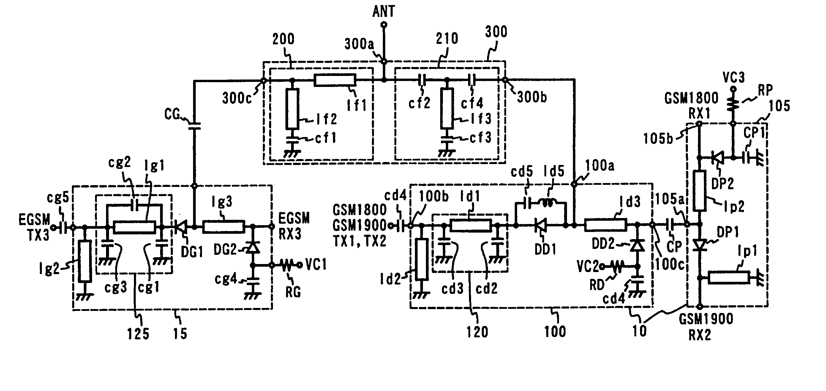
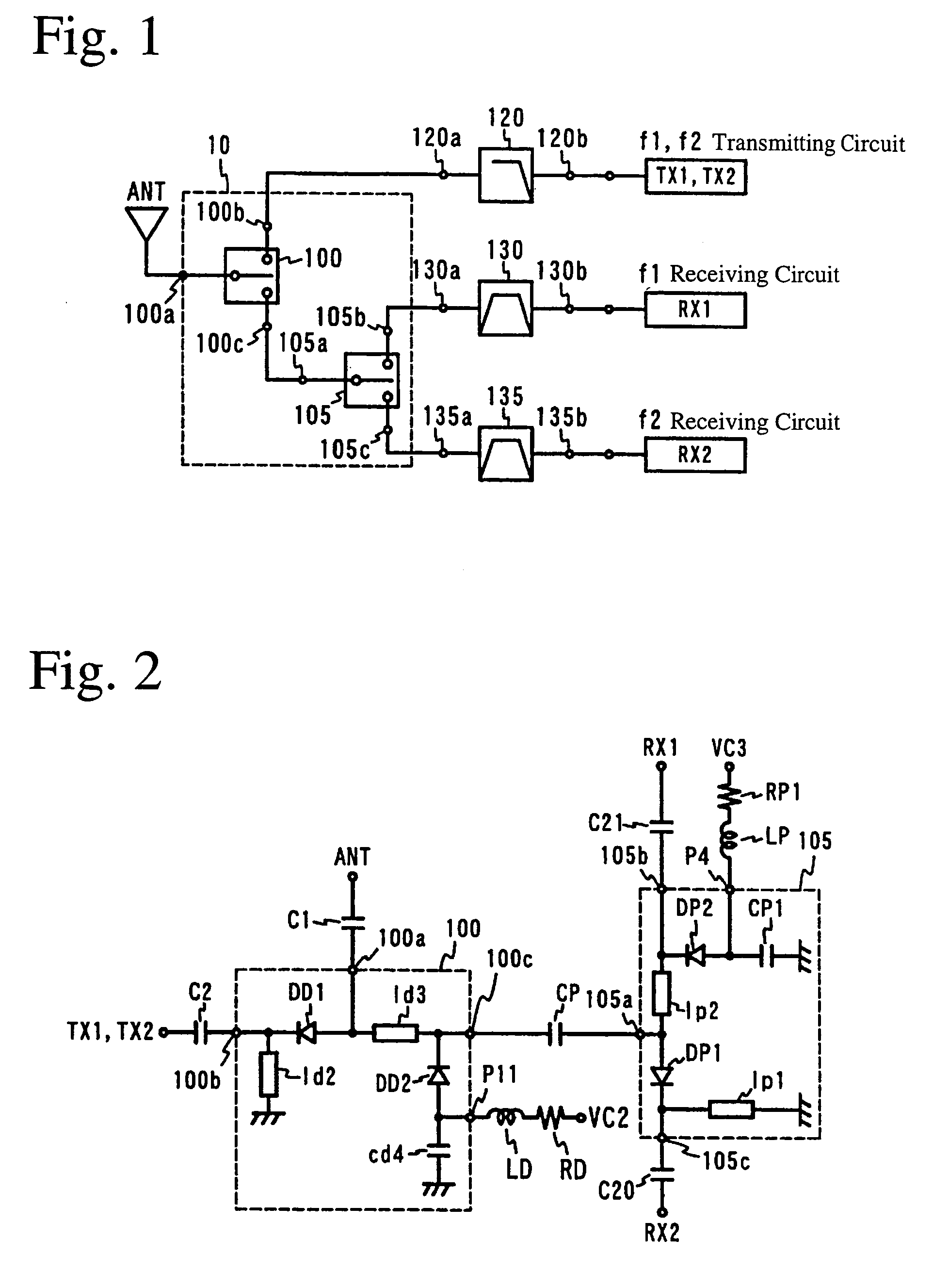
[0048]FIG. 1 shows a high-frequency circuit comprising a switch circuit 10 according to one embodiment of the present invention, and FIG. 2 shows an equivalent circuit of the switch circuit 10. For the simplification of explanation, it is assumed that pluralities of communication systems are GSM 1800 (transmitting frequency: 1710–1785 MHz, receiving frequency: 1805–1880 MHz) as a first communication system f1, and GSM 1900 (transmitting frequency: 1850–1910 MHz, receiving frequency: 1930–1990 MHz) as a second communication system f2, though the present invention is of course not restricted thereto.

[0049]This switch circuit 10 comprising switching elements, inductance elements and capacitance elements is constituted by a first switch means 100 and a second switch means 105. The first switch means 100 comprises a first port 100a connected to an antenna circuit, a second port 100b connected to transmitting circuit TX1,TX2 of GSM 1800 and GSM 1900, and a third port ...


PUM


Abstract

A switch circuit for switching the connection of the receiving or transmitting circuits of two communication systems to an antenna circuit, which comprises first and second switch means having two switching elements, the first switch means comprising a first inductance element between a port connected to the antenna circuit and a port connected to the second switch means; the second switch means comprising a second inductance element between a port connected to the first switch means and a port connected to a receiving circuit of a first communication system, and a transmission line constituting the first inductance element having a lower characteristic impedance than that of a transmission line constituting the second inductance element.

Description

FIELD OF THE INVENTION[0001]The present invention relates to a switch circuit for multi-band mobile phones usable in pluralities of communication systems, and a high-frequency composite part comprising it.BACKGROUND OF THE INVENTION[0002]As mobile equipments such as mobile phones, etc. have recently been used by remarkably increasing numbers of users, their functions and services have extremely improved. Portable wireless communication systems include EGSM (extended global system for mobile communications) and GSM 1800 (global system for mobile communications 1800) widely used mostly in Europe, GSM 1900 (global system for mobile communications 1900) widely used in the U.S., and PDC (personal digital cellular system) used in Japan, etc. From the aspect of convenience by users and efficient use of communications facilities, multi-band mobile phones such as dual-band or triple-band mobile phones, which can utilize pluralities of communication systems, have been developed.[0003]A multi-...

Claims


Application Information

Patent Timeline
Patent Type & Authority Patents(United States)
IPC IPC(8): H04B1/06H04B1/40H04B1/44H04B1/48
CPCH04B1/005H04B1/006H04B1/48H04B1/406
Inventor KEMMOCHI, SHIGERUWATANABE, MITSUHIROTAI, HIROYUKI
Owner HITACHI METALS LTD
Learn More