Method for making a front and back conductive substrate

a technology of front and back electrodes and substrates, which is applied in the direction of contact member manufacturing, conductive pattern formation, printed element electric connection formation, etc., can solve the problems of organic substrates with the same pitch, the pitch of through holes cannot be shortened, and the limit to the pitch of through holes. achieve the effect of enhancing the integration density

Inactive Publication Date: 2007-05-29
FUJITSU LTD
View PDF36 Cites 108 Cited by
  • Summary
  • Abstract
  • Description
  • Claims
  • Application Information

AI Technical Summary

Benefits of technology

[0016]Accordingly, it is an object of the present invention to provide an improved and useful front-and-back electrically conductive substrate and a method for manufacturing same, capable of accommodating demand for enhanced integration densities.

Problems solved by technology

However, a disadvantage of ceramic substrates is that there is a limit to how narrow the pitch of the through holes can be made, because the holes are formed by the mechanical process of punching the substrate and therefore the through-hole pitch cannot be made shorter than the distance by which the punch itself is fed onward.
As a result, organic substrates have the same disadvantage that attends ceramic substrates, that is, that the pitch of the through holes cannot be made shorter than the forward feed pitch of the drill.
Moreover, although the drill used in the organic substrate can be made longer and thinner, doing so creates the possibility that the drill bit will break during operation, a possibility that increases as the depth, that is, the aspect, of the through holes increases.
Additionally, there is the problem that the plating process that is performed after the through holes have been formed in the substrate will not completely cover the interior of the through holes, particularly as the aspect of the holes increases.
As a result, some parts of the inner walls of the through holes may go unplated, thus degrading the reliability of the electrical conductivity.
However, either a ceramic substrate or a resin substrate as described above is used for the base substrate on which the thin film circuitry is formed, so the same problem of how to narrow the pitch of the through holes remains.

Method used


Image

  • Method for making a front and back conductive substrate
  • Method for making a front and back conductive substrate
  • Method for making a front and back conductive substrate

Examples


first embodiment

[0060]A description will now be given of the present invention, with reference to the accompanying drawings.

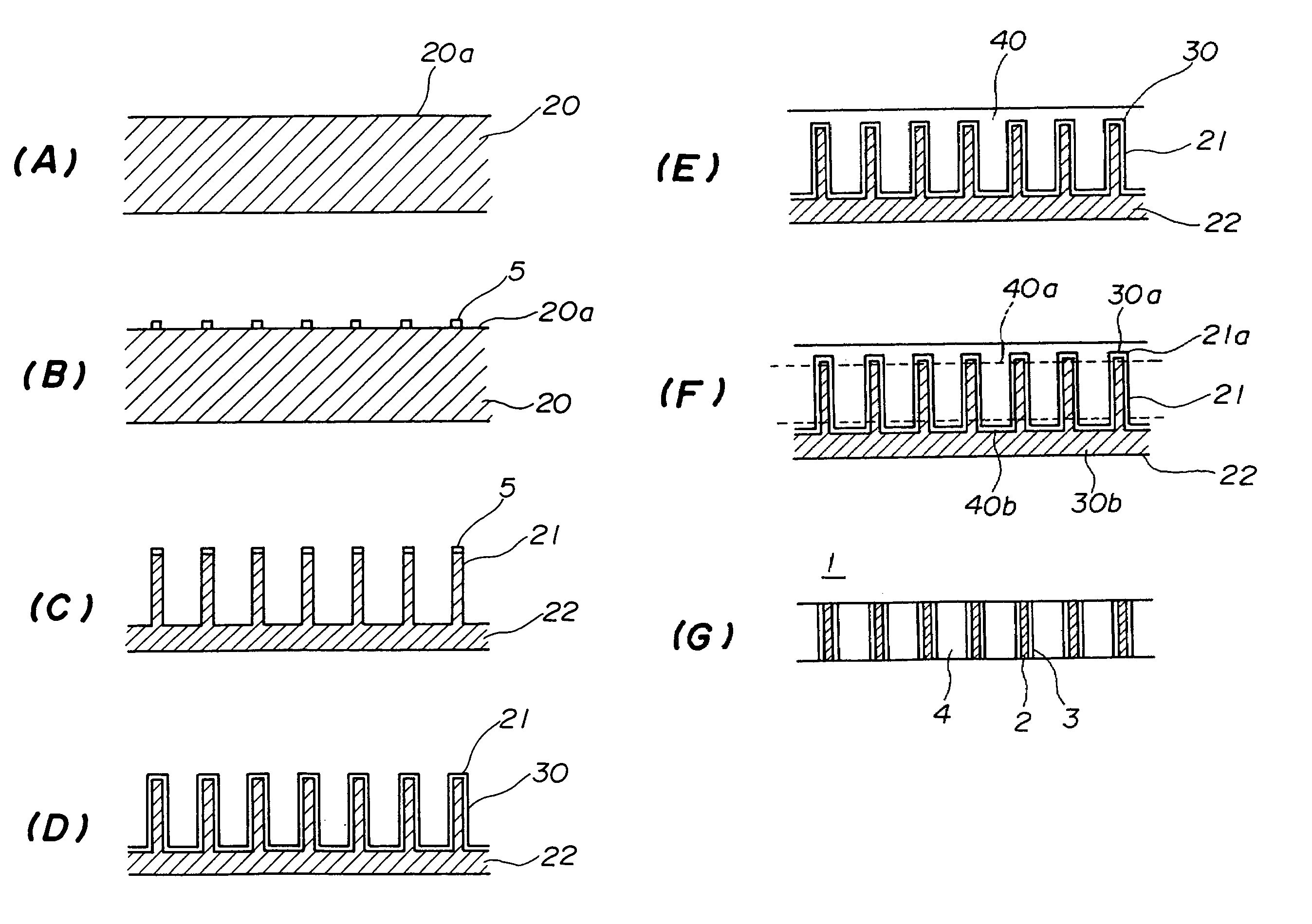
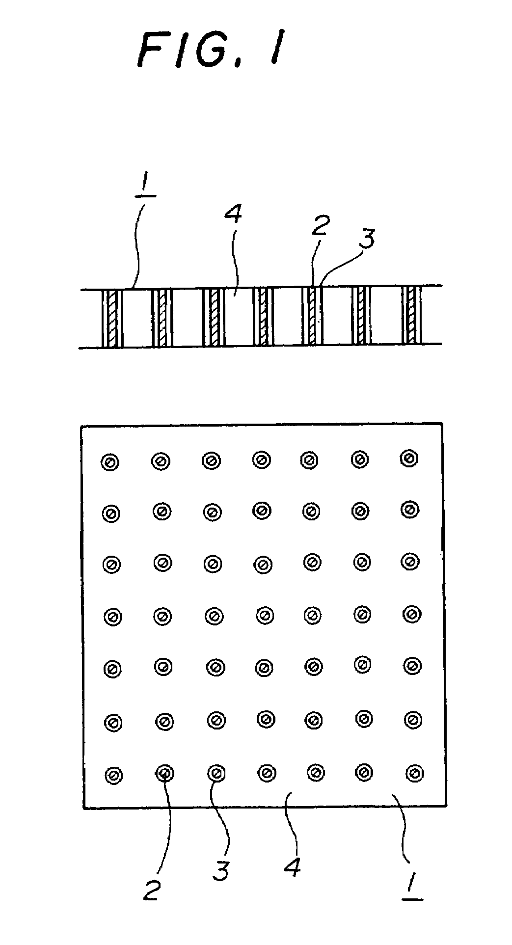
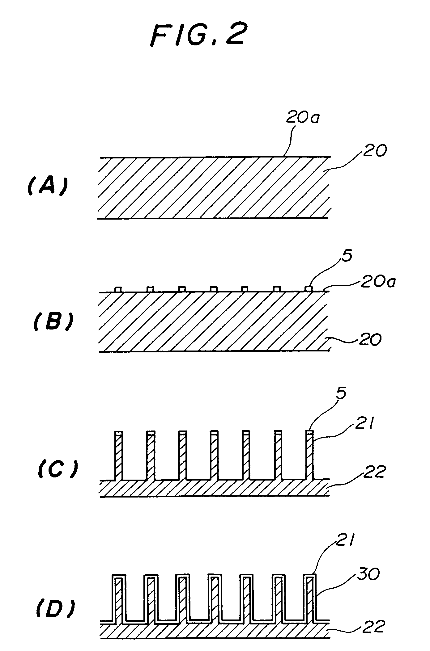
[0061]FIG. 1 shows lateral cross-sectional and plan views of a front-and-back electrically conductive substrate according to a first embodiment of the present invention (hereinafter the first front-and-back electrically conductive substrate). Reference numeral 1 indicates a front-and-back electrically conductive substrate, reference numeral 2 indicates a post, and reference numeral 3 indicates an electrically conductive portion consisting of an electrically conductive film covering a vicinity of a post. The electrically conductive film may be selected as appropriate from among metals such as tungsten, molybdenum, platinum, gold, copper and the like, so long as the metal selected is an electrically conductive metal having a melting point that is higher than the baking temperature of a ceramic-type insulating material to be described later. Reference numeral 4 indicates an insul...


PUM

PropertyMeasurementUnit
aspect ratiosaaaaaaaaaa
heightsaaaaaaaaaa

Abstract

A front-and-back electrically conductive substrate includes a plurality of posts composed of a material that can be anisotropically etched and having an electrically conductive portion that has at least a first surface and a second surface that communicate with each other, and an insulative substrate that supports the plurality of posts.

Description

[0001]This application is a DIVISION of prior application Ser. No. 09 / 783,598 filed Feb. 15, 2001.BACKGROUND OF THE INVENTION[0002]1. Field of the Invention[0003]The present invention relates generally to a front-and-back electrically conductive substrate and a method for manufacturing same, and more particularly, to a high-density front-and-back electrically conductive substrate capable of adapting to the high integration density, increasing post numbers and compactness of the LSIs required for electronic calculators and the like.[0004]2. Description of Related Art[0005]In recent years, the LSI packages and printed wiring boards have needed to acquire ever greater densities as the LSIs and other semiconductor components have become more highly integrated and equipped with a larger number of posts.[0006]With the LSI packages, the LSI chip is mounted face down on a ceramic substrate or an organic substrate. Further, the ceramic substrate or organic substrate is mounted on a printed w...

Claims


Application Information

Patent Timeline
Patent Type & Authority Patents(United States)
IPC IPC(8): H05K3/36H01L21/48H01L23/12H01L23/15H01L23/48H01L23/498H05K1/02H05K1/11H05K3/06H05K3/40H05K3/46
CPCH01L21/486H01L23/49822H01L23/49827H01L23/49833H05K1/0222H05K3/4038H05K3/4602H01L23/481H01L23/147Y10T29/49204H01L2223/6622H01L2924/01078H01L2924/01079H01L2924/09701H01L2924/15311H01L2924/15312H01L2924/3011H05K1/115H05K3/06H05K2201/09809H05K2203/0369H01L2224/73204H01L2924/10253Y10T29/49126H01L2224/16235Y10T29/49165Y10T29/49155Y10T29/49222H01L2924/00H01L2924/00014H01L2224/0401
Inventor MORIIZUMI, KIYOKAZU
Owner FUJITSU LTD
Why Eureka
Try Eureka