

Manufacturing method of semiconductor device suppressing short-channel effect
a manufacturing method and short-channel effect technology, applied in the field of semiconductor devices, can solve the problems of preventing the so-called short-channel effect, limiting the application of the technology, and preventing the development of the structure, so as to achieve the suppression of the short-channel effect and prevent the degradation of the mobility. , the effect of high reliability
- Summary
- Abstract
- Description
- Claims
- Application Information
AI Technical Summary
Benefits of technology
Problems solved by technology
Method used
Image

Examples
Embodiment Construction
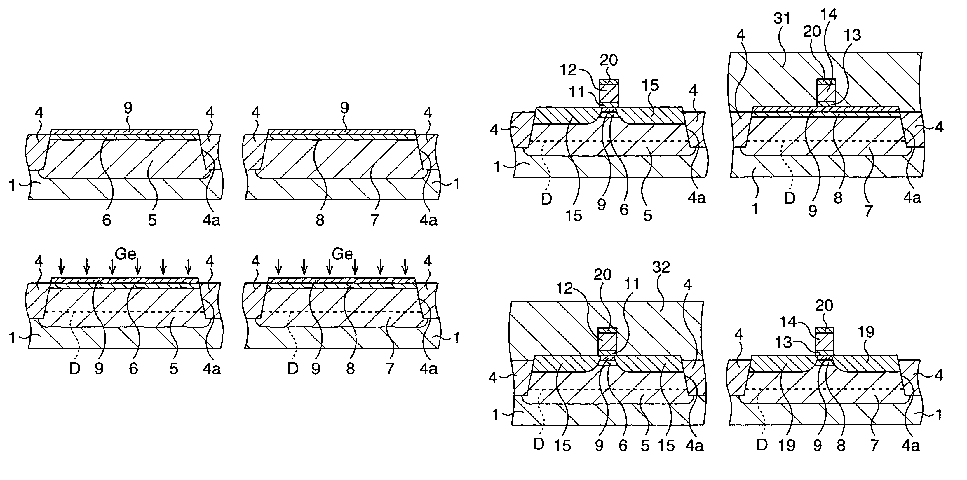
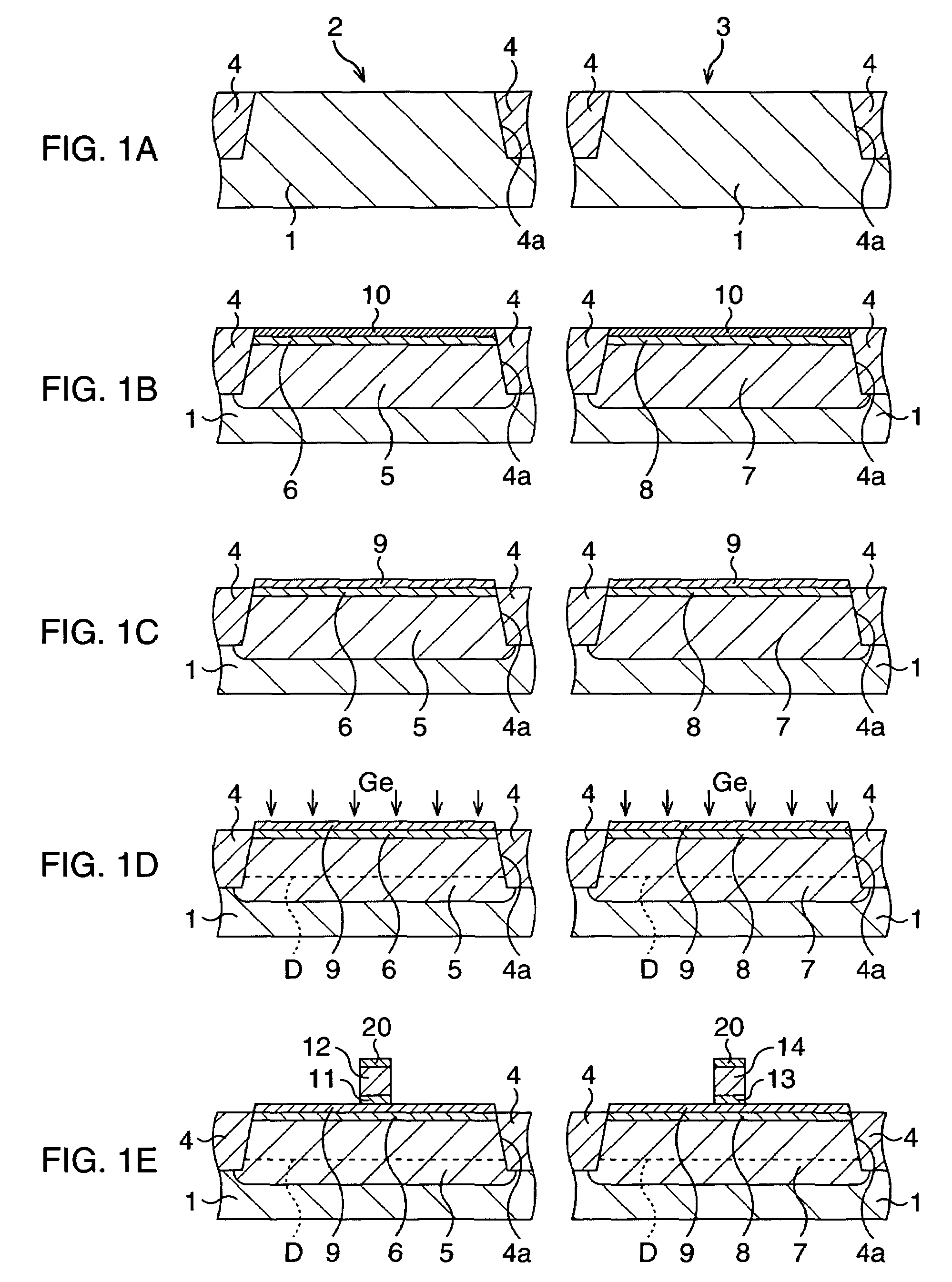
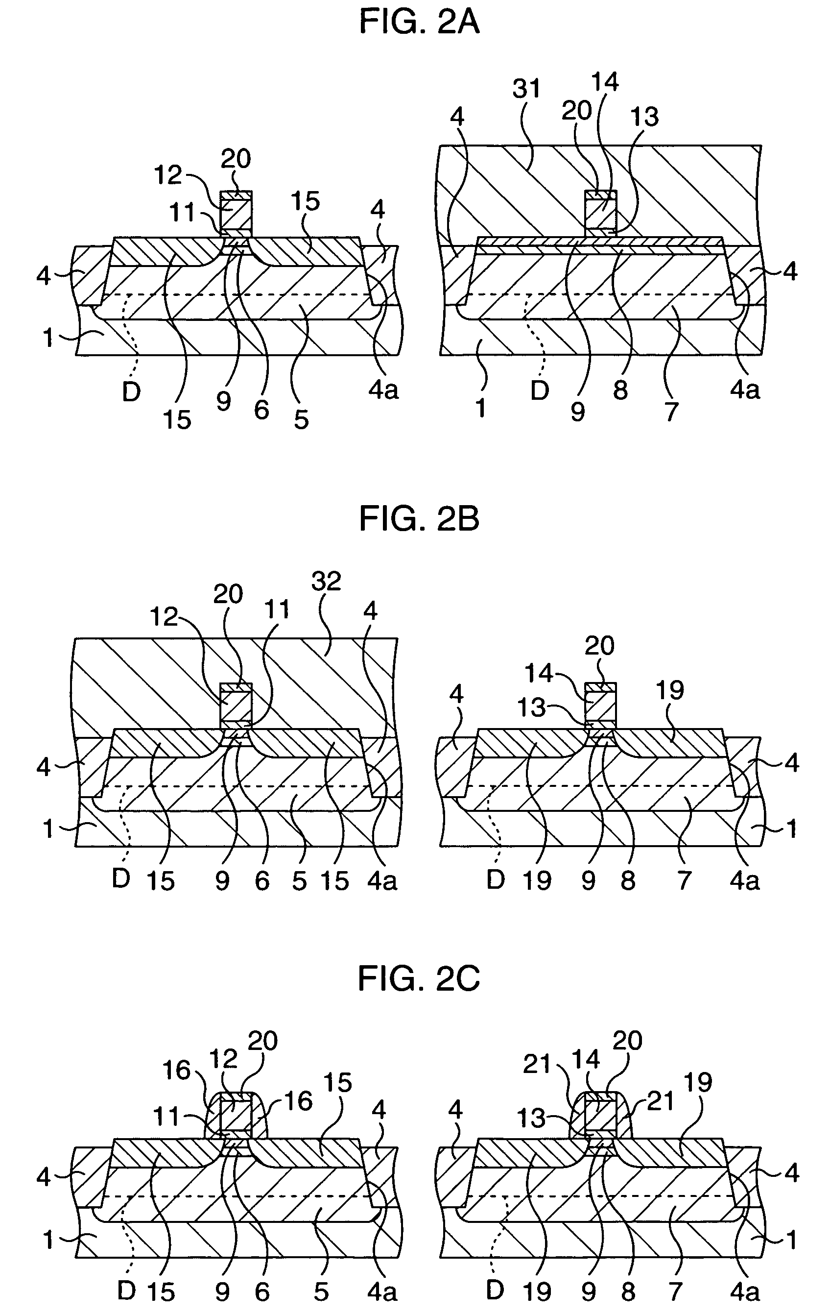
[0018]Basic Gist of the Present Invention
[0019]The inventor, having made every endeavor for easily and reliably realizing an ideal step-profile in the channel region, devised the present invention as follows.
[0020]First, in order to guarantee a generally complete step-profile condition as the initial state, impurities are introduced into the semiconductor region of a substrate, a channel diffusion layer is formed, and subsequently an impurity-free semiconductor film which is to be the surface layer of the channel region is formed on the channel diffusion layer by a selective epitaxial growth or the like.
[0021]Given the above-mentioned initial state, it is necessary to prevent diffusion of impurities by keeping the processing temperature relatively low, in order to maintain the generally complete step-profile of the initial state during the manufacturing process. Among the processes, heat treatment for activating the impurities introduced in the source region and the drain region (an...
PUM
 Abstract
Description
Claims
Application Information