Segmented radiation detector with side shielding cathode

a technology of side shielding cathode and radiation detector, which is applied in the direction of radiation controlled devices, instruments, sustainable manufacturing/processing, etc., can solve the problems of current unfavorable technology implementation, and achieve the effect of reducing electronic noise and good detector energy resolution

Active Publication Date: 2007-05-29
REDLEN TECH
View PDF14 Cites 44 Cited by
  • Summary
  • Abstract
  • Description
  • Claims
  • Application Information

AI Technical Summary

Benefits of technology

[0018]A radiation detector design and method are provided that solve the edge pixel performance problem in pixilated radiation detectors, without the use of multi-electrode or other presently known correction methods, and avoid drawbacks associated with those correction techniques. Further, the designs are practical for manufacturing. The embodiments of detector and electrode design demonstrate that the resulting device leakage current, the surface leakage current in particular, is not increased to an excessive level as often observed with multi-electrode designs. The leakage current of the embodiments minimize electronic noise and provide good detector energy resolution, especially of the edge pixels. Additionally, for the case of CZT pixilated detectors, applications in X-ray imaging are enabled. The low level leakage current allows the operation of the device at high bias voltages (>>200V / mm or >>1000V / 5 mm)—a condition required in X-ray imaging applications, (especially medical imaging), which is believed to be currently unfeasible to achieve with existing technologies.

Problems solved by technology

The low level leakage current allows the operation of the device at high bias voltages (>>200V / mm or >>1000V / 5 mm)—a condition required in X-ray imaging applications, (especially medical imaging), which is believed to be currently unfeasible to achieve with existing technologies.

Method used


Image

  • Segmented radiation detector with side shielding cathode
  • Segmented radiation detector with side shielding cathode
  • Segmented radiation detector with side shielding cathode

Examples


exemplary embodiment performance

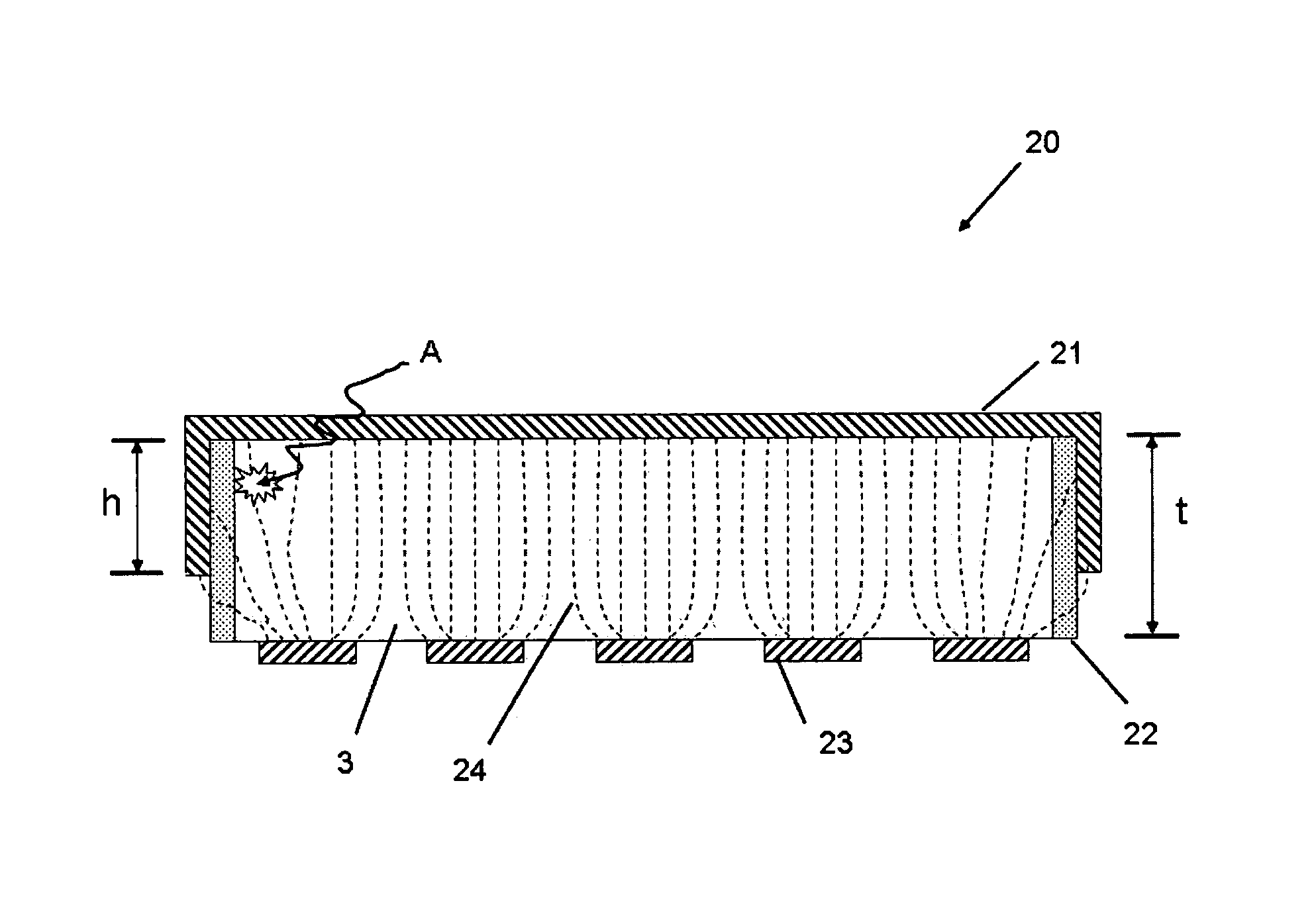
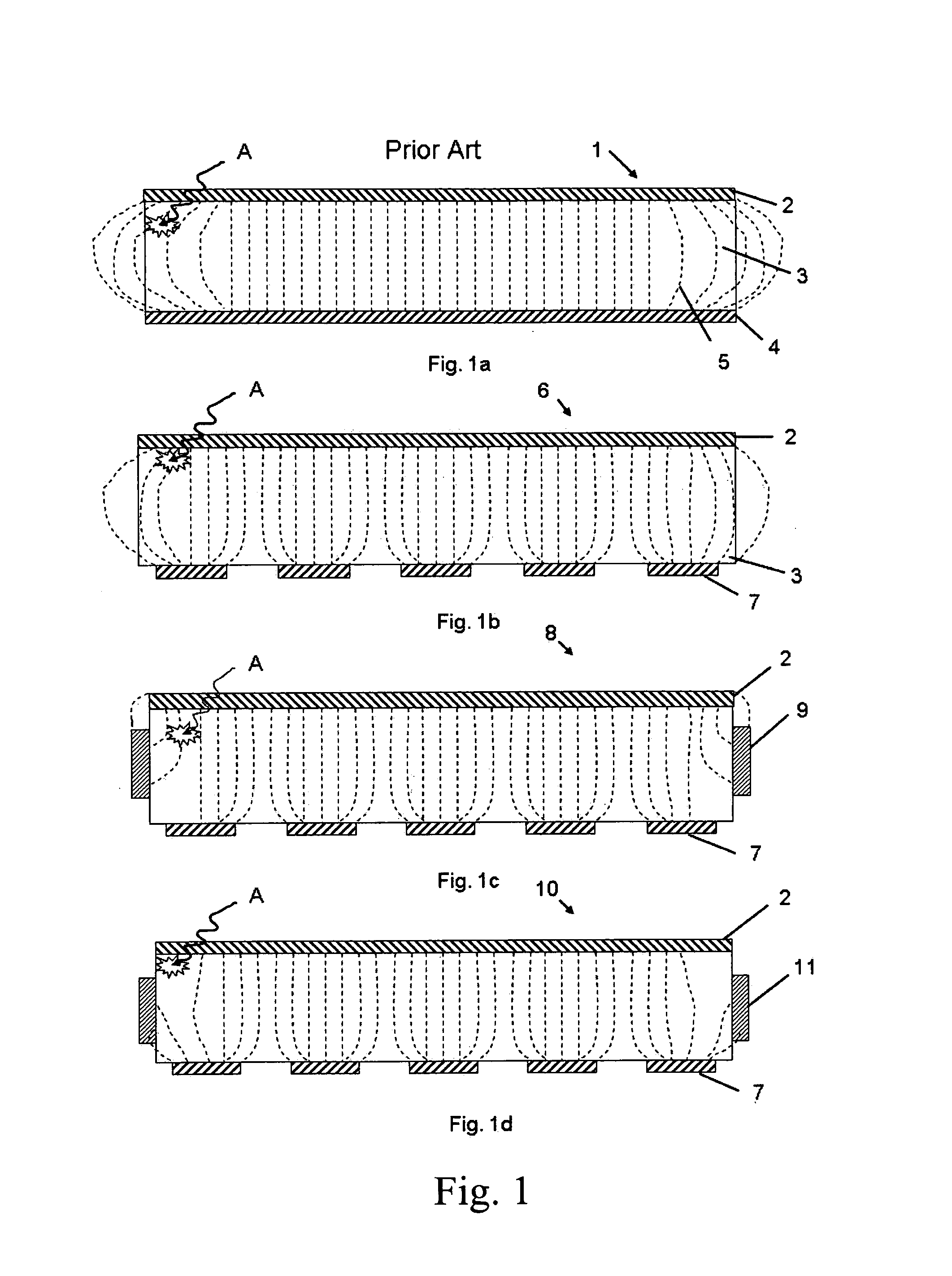
[0059]The previous unshielded results are compared to a radiation detector with the modification of side-shielded cathode embodiment of FIG. 9, with test results as shown in FIG. 7. The CZT detector configuration corresponded to the conventional baseline example for array and tile dimensions. Tile thickness was 5 mm, the anode array was 10×10 pixels, and the electrodes were gold, and the side insulator was Humiseal polymer, and the side portion extends 2.5-3 mm. The radiation source was Co-57; radiation energy 122 keV, bias voltage 500V. In general, a dramatic improvement in the FWHM energy spike on the outer pixels is demonstrated with improved peak counts. Both of these measures improve signal to noise and quality of derived signal. Improvements in charge collection efficiency result in improvements in both energy resolution and peak counting efficiency, as shown. The side-shielding cathode detector improves both outer corner pixels (typically affected the most by shielding) and a...


PUM


Abstract

A semiconductor radiation detector is provided for improved performance of pixels at the outer region of the crystal tile. The detector includes a semiconductor single crystal substrate with two major planar opposing surfaces separated by a substrate thickness. A cathode electrode covers one of the major surfaces extending around the sides of the substrate a fraction of the substrate thickness and insulated on the side portions by an insulating encapsulant. An exemplary example is given using Cadmium Zinc Telluride semiconductor, gold electrodes, and Humiseal encapsulant, with the side portions of the cathode extending approximately 40-60 percent of the substrate thickness. The example with CZT allows use of monolithic CZT detectors in X-ray and Gamma-ray applications at high bias voltage. The shielding electrode design is demonstrated to significantly improve gamma radiation detection of outer pixels of the array, including energy resolution and photopeak counting efficiency. The detector has performance of detector leakage current density less than 6 nA/mm2 at a bias potential of substantially 1400V, and responsive to gamma radiation such that the energy resolution full width half maximum of more than 90% of the pixels is less than 6%.

Description

TECHNICAL FIELD[0001]The present invention relates to the field of radiation detectors and, more particularly, to detector assemblies employed for X-Ray and Gamma ray imaging.BACKGROUND OF THE INVENTION[0002]High-resistivity semiconductor radiation detectors are widely used for detecting ionizing radiation due to their ability to operate at room temperature, their small size and durability, and other features inherent in semiconductor devices. Such detectors are used in a wide variety of applications, including medical diagnostic imaging, nuclear waste monitoring, industrial process monitoring, and space astronomy. Ionizing radiation includes both particulate radiation, such as alpha or beta particles, and electromagnetic radiation such as gamma or x rays.[0003]Conventional semiconductor radiation detectors can be configured in several types, for example, planar or monolithic. The simplest form is a planar detector 1 which includes a semiconductor crystal 3 located between cathode 2...

Claims


Application Information

Patent Timeline
Patent Type & Authority Patents(United States)
IPC IPC(8): G01T1/24G01T1/29H01L31/0203H01L31/18H01L31/0224
CPCG01T1/2928H01L27/14676H01L27/14696H01L31/085H01L31/1828H01L2924/0002Y02E10/543H01L2924/00G01T1/241Y02P70/50
Inventor CHEN, HENRYAWADALLA, SALAH
Owner REDLEN TECH
Why Eureka
Try Eureka