
Method for enhancing FSG film stability

a technology of enhancing the stability of fsg, which is applied in the direction of semiconductor devices, semiconductor/solid-state device details, electrical apparatus, etc., can solve the problems of increasing the importance of wiring in the circuit, the tendency of copper to diffuse quickly, and the inability to rely on materials to serve as a barrier against copper diffusion, etc., to achieve the effect of preventing fluorine outward diffusion and enhancing the stability of th

Inactive Publication Date: 2007-06-05
TAIWAN SEMICON MFG CO LTD
View PDF35 Cites 0 Cited by
  • Summary
  • Abstract
  • Description
  • Claims
  • Application Information

AI Technical Summary

Benefits of technology

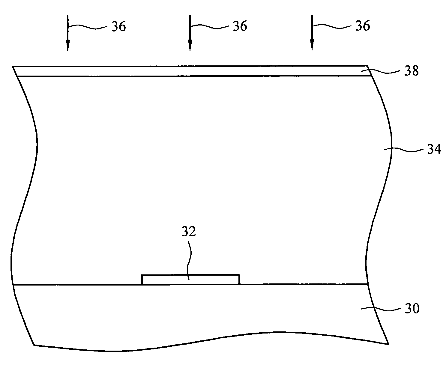
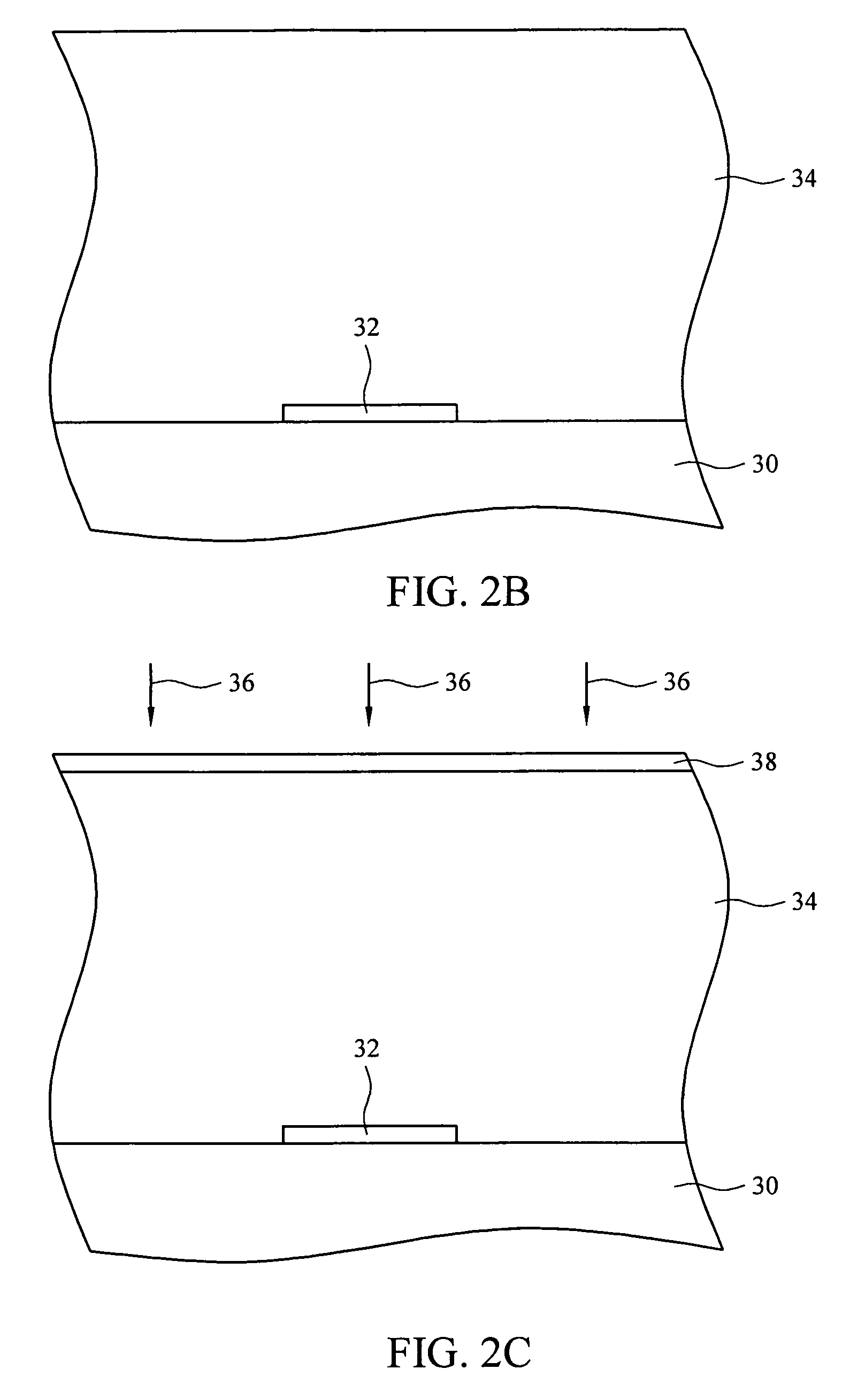
[0018]In accordance with these and other objects and advantages, the present invention is generally directed to a novel method for enhancing stability of an FSG layer. In one embodiment, the method is an in-situ method which is carried out typically in a CVD chamber after formation of the FSG layer on a substrate. The method includes depositing the FSG layer on the substrate and introducing a phosphorous and hydrogen-containing gas, preferably phosphine (PH3), into the chamber. The phosphine dissociates into reactive hydrogen and phosphorous species. The reactive hydrogen species can scavenge fluoride radicals to produce hydrogen fluoride (HF) gas, which is evacuated from the chamber. The reactive phosphorous species react with oxygen to form a phosphorous oxide (PSG) film on the FSG layer. An oxide-like (PSG) film was, thus, formed on top of FSG and / or neighboring with the FSG on the trench sidewall would play a role of blocking layer to prevent fluorine outward diffusion. On the other hand, by gettering moisture and mobile ions in the chamber, the PSG film prevents fluoride-based radicals from attacking and damaging the FSG layer.

Problems solved by technology

As integrated circuits decrease in size, delays associated with the wiring in the circuits have become increasingly important.
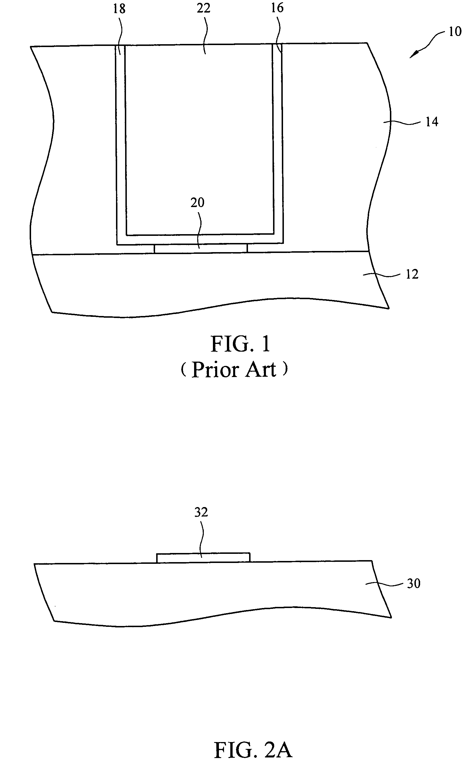
One of the problems associated with the use of copper in copper interconnect is the tendency of copper to diffuse quickly and serve as a source of recombination centers in silicon.
However, these materials cannot be relied upon to serve as a barrier against copper diffusion when conventional multi-layering is used due to the difficulty of using the materials to cover the edges of the wiring.
These could have a tendency that contains Fluorine reactive gases and / or radical to chemically attack and / or to form the defects on the deposited FSG layer as well as subsequent processes, ex., forming the metal structures in devices being fabricated on the wafer, resulting in the instabilities in the devices.

Method used


Image

  • Method for enhancing FSG film stability
  • Method for enhancing FSG film stability
  • Method for enhancing FSG film stability

Examples


first embodiment

[0045]A flow diagram which summarizes sequential process steps carried out according to the ex-situ method for enhancing FSG film stability according to the present invention is shown in FIG. 6. In step 1, an FSG layer is provided on a substrate. In step 2, a via opening is etched in the FSG layer. In step 3, the via opening is cleaned, typically using fluorine-based solvents. In step 4, the FSG layer is exposed to a phosphorous- and hydrogen-containing gas, preferably PH3 and N2O.

second embodiment

[0046]FIG. 7 illustrates a flow diagram which summarizes sequential process steps carried out according to the ex-situ method for enhancing FSG film stability according to the present invention. In step 1a, a metal via is provided in an FSG layer provided on a substrate. In step 2a, the metal via is subjected to CMP to remove metal overburden from the via. In step 3a, the FSG layer is exposed to a phosphorous- and hydrogen-containing gas, preferably PH3 and N2O.


PUM


Abstract

A method for enhancing stability of a fluorinated silicon glass layer is disclosed. A fluorinated silicon glass layer provided on a substrate is subjected to a phosphorous-containing and hydrogen-containing gas such as phosphine (PH3), for example. The gas forms reactive hydrogen species which removes fluorine radicals and reactive phosphorous species which forms a moisture-gettering and ion-gettering phosphorious oxide film the layer.

Description

FIELD OF THE INVENTION[0001]The present invention relates to intermetal dielectric (IMD) layers formed in the fabrication of semiconductor devices. More particularly, the present invention relates to a method for enhancing the stability of a fluorinated silicon glass (FSG) layer in semiconductor device fabrication by introducing a hydrogen-containing gas with an oxygen-containing gas into a process chamber immediately after the formation of the FSG layer in order to remove free fluorine radicals and reactive fluorine-based gases from the chamber.BACKGROUND OF THE INVENTION[0002]The fabrication of various solid state devices requires the use of planar substrates, or semiconductor wafers, on which integrated circuits are fabricated. The final number, or yield, of functional integrated circuits on a wafer at the end of the IC fabrication process is of utmost importance to semiconductor manufacturers, and increasing the yield of circuits on the wafer is the main goal of semiconductor fa...

Claims


Application Information

Patent Timeline
Patent Type & Authority Patents(United States)
IPC IPC(8): H01L21/316H01L21/473
CPCH01L21/02129H01L21/02131H01L21/022H01L21/02211H01L21/02274H01L21/3105H01L21/31629H01L21/76801H01L21/76826H01L21/76829H01L21/76831H01L21/76834
Inventor TSAI, CHENG-YUANCHOU, YOU-HUALIN, CHIH-LUNG
Owner TAIWAN SEMICON MFG CO LTD
Learn More