Data output device and method of semiconductor device

a data output device and semiconductor technology, applied in the direction of logic circuit coupling/interface arrangement, pulse technique, instruments, etc., can solve the problems of inability to secure sufficient address access time margin, difficult to acquire an adequate bandwidth for data transfer to an input/output stage, and increased power noise of memory devices. , to achieve the effect of accurately and stably processing high-speed data and reducing power nois

Active Publication Date: 2007-06-05
SK HYNIX INC
View PDF6 Cites 8 Cited by
  • Summary
  • Abstract
  • Description
  • Claims
  • Application Information

AI Technical Summary

Benefits of technology

[0010]Therefore, the present invention has been made in view of the above problems, and it is an object of the present invention to provide a data output device and method of a semiconductor device which can reduce power noise in an output driver resulting from a data transition when data is outputted from the semiconductor device, can accurately and stably process high-speed data in a high-frequency operation of the semiconductor device, and can normally output data even though a no-operation period is generated in a series of data output operations.

Problems solved by technology

However, recently, as the demand for the high-speed operation of a processor such as a central processing unit (CPU) or graphics processing unit (GPU) increases rapidly, the low-power / high-speed operation of the memory device has been increasingly required.
However, because of power noise and switching noise resulting from a switching operation with respect to data, it is not easy to acquire an adequate bandwidth for data transferred to an input / output stage.
In this regard, it has also become a very important issue to enable a high-speed input / output operation along with the high-frequency operation.
However, the above-mentioned conventional DBI-based data output method is disadvantageous in that a sufficient address access time margin cannot be secured and high-speed data cannot be accurately and stably processed in a high-frequency operation.
For this reason, only when at least a period of 5 clk to 8 clk must be guaranteed, is the data output enabled (see FIG. 2), thereby making it difficult to secure an adequate data access time margin and consuming a relatively large amount of time in processing data.
In conclusion, the conventional DBI-based data output method has the disadvantage of not only being hard to apply and implement for the high-frequency operation, but also being inappropriate to the accurate and stable processing of high-speed data.

Method used


Image

  • Data output device and method of semiconductor device
  • Data output device and method of semiconductor device
  • Data output device and method of semiconductor device

Examples


Embodiment Construction

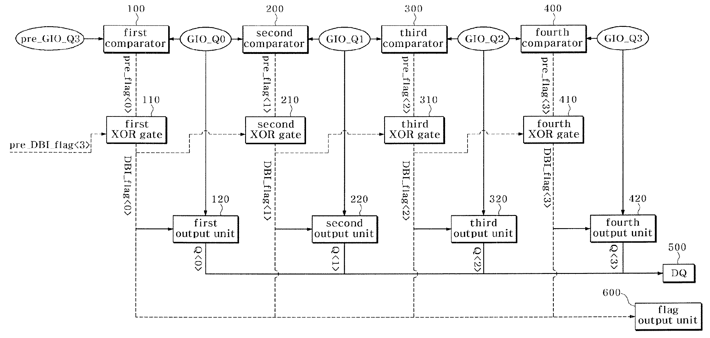
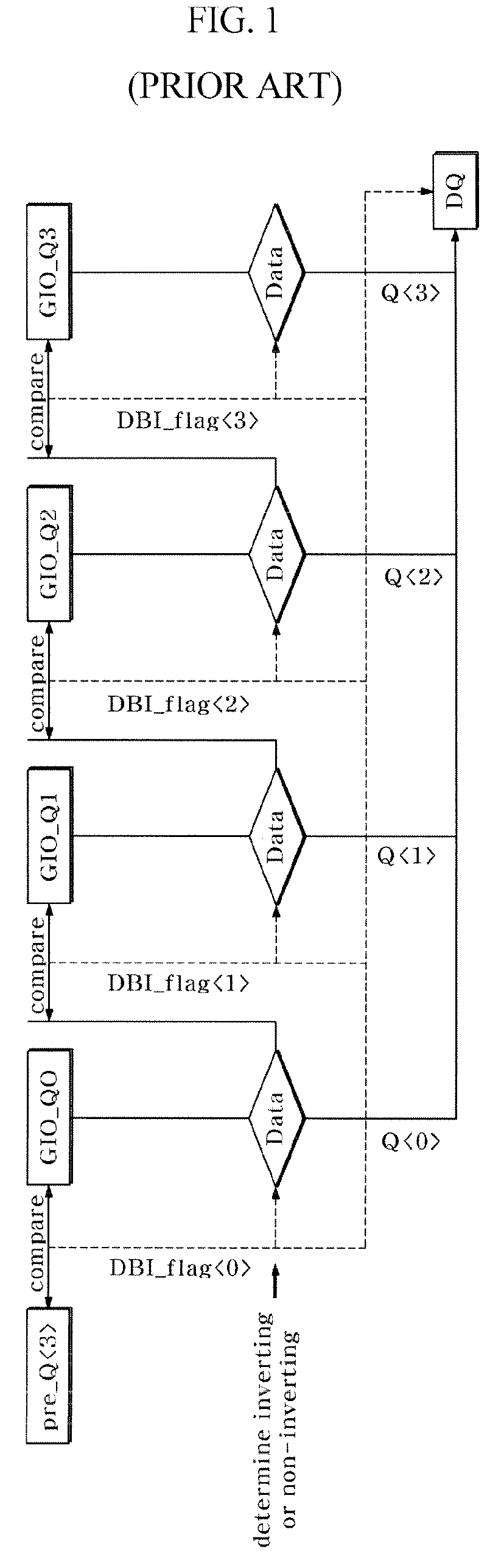
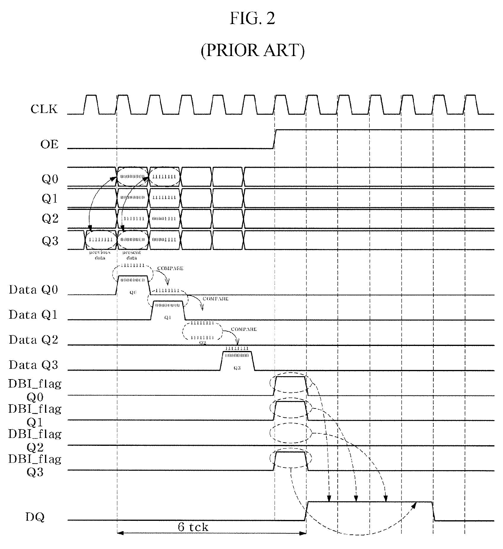
[0055]FIG. 3 shows the configuration of a data output device of a semiconductor device according to the present invention, FIG. 4 shows the configuration of a comparator in the data output device according to the present invention, FIG. 5 shows the configuration of a sub-output unit in the data output device according to the present invention, FIG. 6 is a timing diagram of signals in a data output method of a semiconductor device according to the present invention, FIG. 7 shows the configuration of an output data initializer in the data output device according to the present invention, FIG. 8 shows the configuration of an initialization signal generator in the data output device according to the present invention, and FIG. 9 shows the configuration of a flag initializer in the data output device according to the present invention. The preferred embodiments of the present invention will hereinafter be described with reference to the figures.

[0056]The data output device of the semicon...


PUM


Abstract

A data output device is disclosed having a first comparator for comparing first output data with arbitrary output data on a bit-by-bit basis and outputting a first pre-flag signal, a second comparator for comparing second output data with the first output data on a bit-by-bit basis and outputting a second pre-flag signal, first and second logic units for performing logic operations with respect to pre-flag signals and data inversion flag signals, a first output unit for inverting or non-inverting and outputting a plurality of bits contained in the first output data in response to the first data inversion flag signal, a second output unit for inverting or non-inverting and outputting a plurality of bits contained in the second output data in response to the second data inversion flag signal, and an output data initializer for, when a no-operation period is generated in a series of data output operations, initializing the arbitrary output data and supplying the resulting data to the first comparator.

Description

CROSS REFERENCE TO RELATED APPLICATIONS[0001]This application relies for priority upon Korean Patent Application No. 2005-60596 filed on Jul. 6, 2005, the contents of which are herein incorporated by reference in their entirety.FIELD OF THE INVENTION[0002]The present invention relates to a data output device and method of a semiconductor device, and more particularly to a data output device and method of a semiconductor device which can reduce power noise in an output driver resulting from a data transition when data is outputted from the semiconductor device and can accurately and stably process high-speed data even though a no-operation period is generated in a series of data output operations.DESCRIPTION OF THE RELATED ART[0003]With the continuous advance of a semiconductor memory device, a variety of new operating systems have recently been proposed to process data at high speed. The semiconductor memory device is adapted to perform a write / read operation based on the operation ...

Claims


Application Information

Patent Timeline
Patent Type & Authority Patents(United States)
IPC IPC(8): G06F3/00H03K19/0175
CPCG11C7/02G11C7/1006G11C7/1051G11C7/1069G11C7/20H03M9/00G11C7/106
Inventor KWACK, SEUNGKWEAN, KI
Owner SK HYNIX INC
Why Eureka
Try Eureka