Radiation detector

a detector and radiofrequency technology, applied in the field of radiofrequency detectors, can solve the problems of low-quality radiographic images, defects that cannot be long-term reliable, and could occur, and achieve the effect of improving the bonding property of the common electrod

Inactive Publication Date: 2007-06-19
SHIMADZU CORP
View PDF7 Cites 2 Cited by
  • Summary
  • Abstract
  • Description
  • Claims
  • Application Information

AI Technical Summary

Benefits of technology

[0011]This invention has been made having regard to the state of the art noted above, and its object is to provide a radiation detector that can suppress a generation of defects in an amorphous selenium semiconductor film resulting from lamination thereon of a common electrode for bias voltage application, and can improve the bonding property of the common electrode.

Problems solved by technology

However, the conventional radiation detector with the above construction has a drawback that defects could occur with the radiation sensitive a-Se semiconductor film 52 when the a-Se semiconductor film 52 is damaged by the heat of vapor deposition for forming the common electrode 53 for bias voltage application on the a-Se semiconductor film 52.
The a-Se semiconductor film 52 with many defects lacks in long-term reliability, and detection errors caused by the defects result in low-quality radiographic images.
Further, the conventional radiation detector has a drawback of being low in bonding strength between the radiation sensitive a-Se semiconductor film 52 and common electrode 53 for bias voltage application.
Where an aluminum or MgAg film of about 100 nanometers (nm) (=1,000 angstroms) is used, the common electrode 53 has a weak bonding strength, and hence low reliability.

Method used


Image

  • Radiation detector
  • Radiation detector
  • Radiation detector

Examples


second embodiment

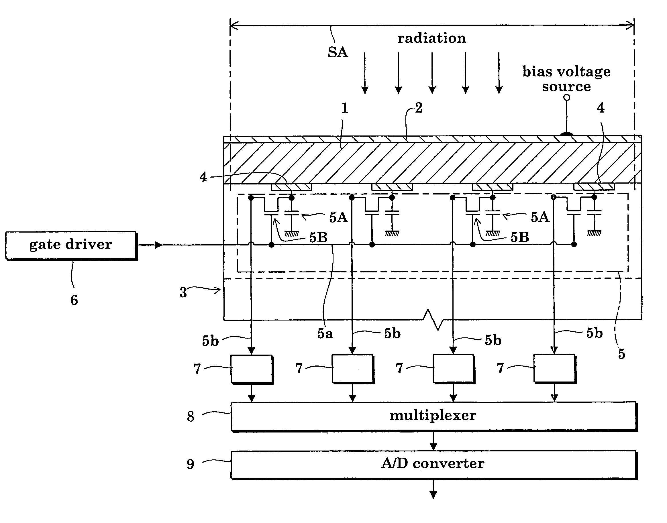
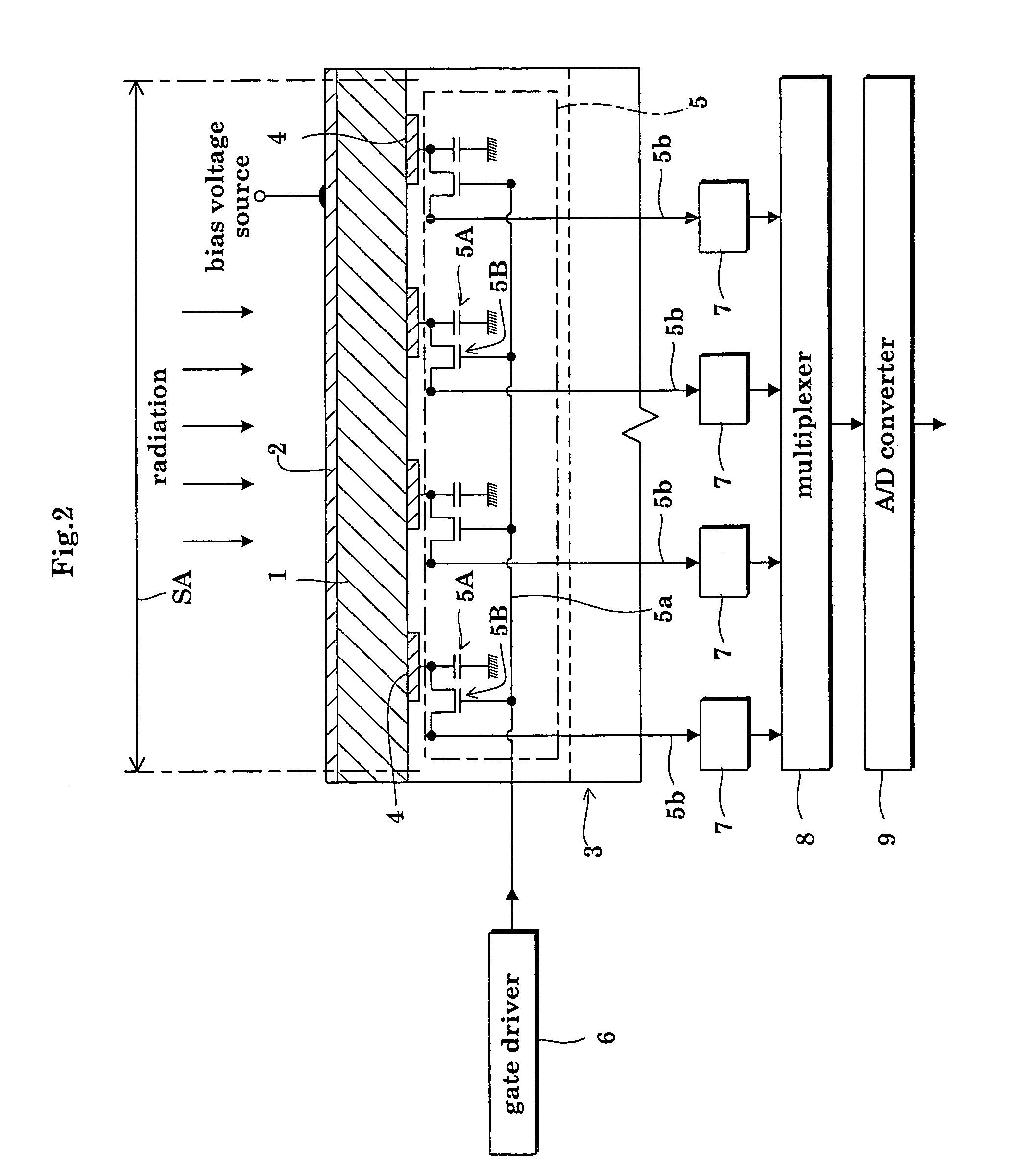
[0063]A radiation detector in a second embodiment will be described with reference to the drawings. FIG. 4 is a block diagram showing, in section, a principal portion of a radiation detector of the direct conversion type in the second embodiment of the invention.

[0064]As shown in FIG. 4, the radiation detector in the second embodiment includes a carrier selective intermediate layer 10 formed between the a-Se semiconductor film 1 and common electrode 2, and a carrier selective intermediate layer 11 formed between the a-Se semiconductor film 1 and collecting electrodes 4. The other aspects are the same as in the detector in the first embodiment. Only different features will be described below, and the common features will not be described again.

[0065]The detector in the second embodiment, with the carrier selective intermediate layers 10 and 11, can reduce dark current. The detector in the second embodiment has the common electrode 2 formed on the carrier selective intermediate layer ...


PUM


Abstract

The radiation detector according to this invention has a common electrode for bias voltage application formed on a surface of an amorphous selenium semiconductor film (a-Se semiconductor film) sensitive to radiation. The common electrode is a gold thin film having a thickness in a range of 100 to 1,000 Å. The gold thin film acting as the common electrode may be formed on the surface of the a-Se semiconductor film at a relatively low vapor deposition temperature and in a reduced vapor deposition time. This feature suppresses a generation of defects in the a-Se semiconductor film due to formation of the common electrode. The gold thin film for the common electrode is not so thick as in the prior art, but is 1,000 Å or less. With the reduced thickness, the common electrode has improved boding property with respect to the a-Se semiconductor film.

Description

BACKGROUND OF THE INVENTION[0001](1) Field of the Invention[0002]This invention relates to radiation detectors of the direct conversion type including an amorphous selenium semiconductor film (hereinafter referred to as “a-Se semiconductor film” where appropriate) sensitive to radiation, for use in the medical, industrial, nuclear and other fields.[0003](2) Description of the Related Art[0004]An indirect conversion type radiation detector first converts radiation (e.g. X rays) into light, and then converts the light into electric signals by photoelectric conversion. As distinct from the indirect conversion type, a direct conversion type radiation detector converts incident radiation (e.g. X rays) directly into electric signals (charges) by an a-Se semiconductor film sensitive to radiation. FIG. 1 is a schematic sectional view showing a basic construction of a conventional radiation detector of the direct conversion type.[0005]The radiation detector shown in FIG. 1 includes an active...

Claims


Application Information

Patent Timeline
Patent Type & Authority Patents(United States)
IPC IPC(8): G01T1/00A61B6/00G01J1/02G01T1/24H01L27/14H01L27/146H01L31/0224H01L31/08H01L31/09H01L31/115
CPCH01L27/14676G01T1/24
Inventor WATADANI, KOJISATO, KENJISHIMURA, YOICHIROTSURUTA, HIDEO
Owner SHIMADZU CORP
Why Eureka
Try Eureka