Light propagation structure and optical display device of optical system, light propagation method of optical system, and display method of optical display device

a technology of optical display device and light propagation structure, which is applied in the direction of picture reproducers using projection devices, television systems, instruments, etc., can solve the problems of inability to adequately demonstrate the expressive capabilities of cg images, inability to accurately transmit the optical image of the first optical modulation element to the pixel surfaces of the second optical modulation element, and lack of realism of the display imag

Inactive Publication Date: 2007-06-26
SEIKO EPSON CORP
View PDF9 Cites 16 Cited by
  • Summary
  • Abstract
  • Description
  • Claims
  • Application Information

AI Technical Summary

Benefits of technology

[0062]As a result, the same effect is obtained as that of the optical display device of the eighth invention.

Problems solved by technology

When considering the displayed images of current optical display devices in terms of these vision characteristics, the narrowness of the luminance dynamic range is conspicuous, and due to a lack of gradation of shadowed and highlighted areas, displayed images appear to lack realism and impact.
However, due to the lack of performance of optical display devices that display that data, there is the problem in which CG images are unable to adequately demonstrate their inherent expressive capabilities.
However, in the invention described in Patent Document 1, even though an optical isolator is provided between the first and second optical modulation elements and the first and second optical modulation elements are separated from each other, since there is no lens or other image-forming means between them, there was the problem of it being difficult to accurately transmit the optical image of the first optical modulation element to the pixel surfaces of the second optical modulation element.
In addition, in the invention described in Patent Document 2, although image-forming accuracy can be improved to a certain extent if that having high accuracy is used for the lenses, mirrors and other optical components that compose the illumination optical system, there was the problem of composing with highly accurate optical components leading to increased costs.
However, current optical modulation elements (e.g., liquid crystal light valves) already have pixel densities that approach the upper limit of hyperfine processing technology in order to achieve higher resolution, and in consideration of this point, it would be difficult to attempt to realize a pixel density that is three to five times greater in first optical modulation element 130.
Moreover, since optical images of each element lens are formed on the pixel surfaces of second optical modulation element 140 with only two lenses consisting of fly eye lens 112b and converging lens 12d located far from first optical modulation element 130, aberration is unable to be adequately corrected which inevitably results in considerable blurring of the images.
Accordingly, there was the problem of it being difficult accurately adjust luminance.

Method used


Image

  • Light propagation structure and optical display device of optical system, light propagation method of optical system, and display method of optical display device
  • Light propagation structure and optical display device of optical system, light propagation method of optical system, and display method of optical display device
  • Light propagation structure and optical display device of optical system, light propagation method of optical system, and display method of optical display device

Examples


Embodiment Construction

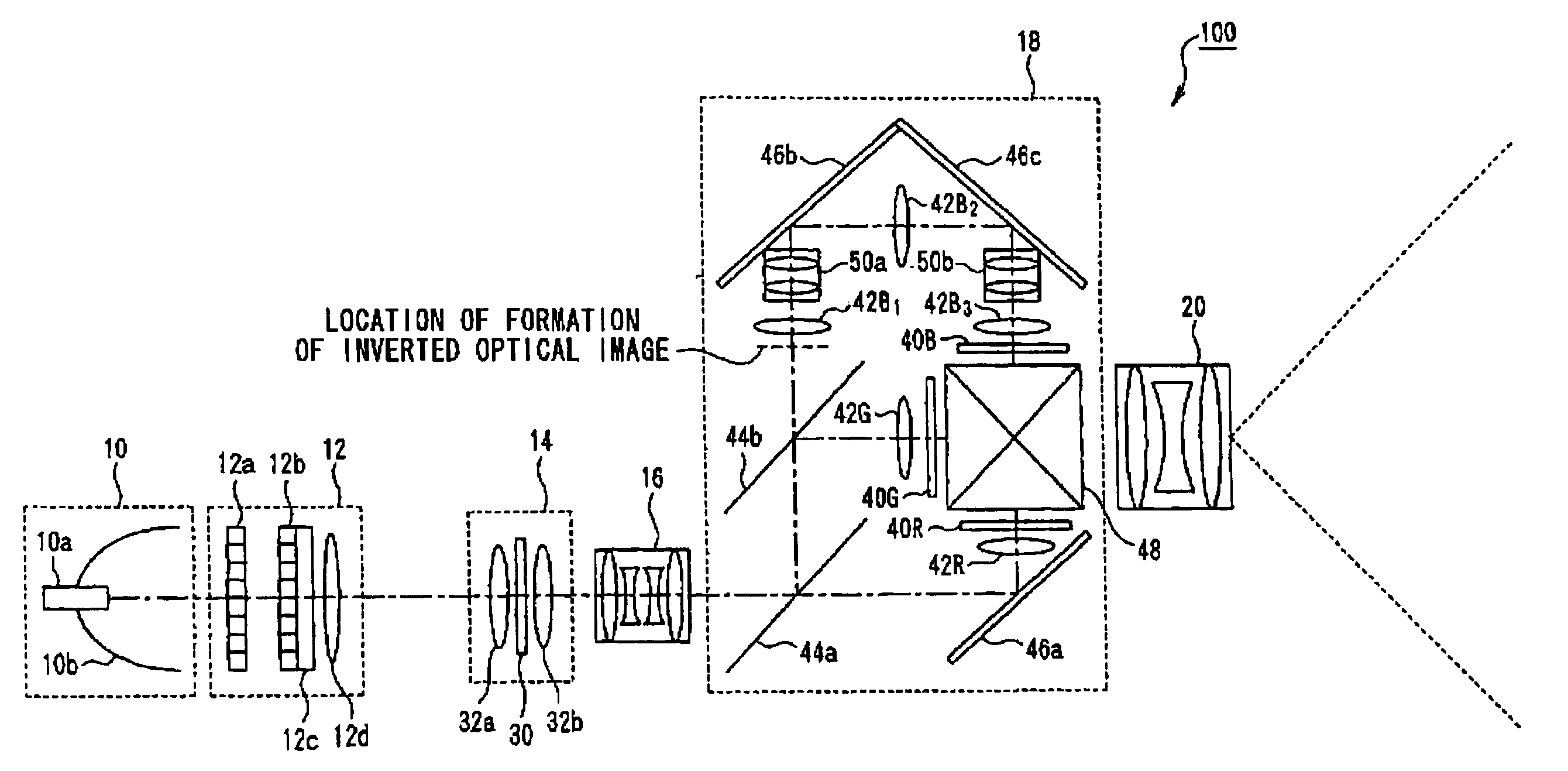
[0086]The following provides an explanation of embodiments of the present invention with reference to the drawings. FIGS. 1 through 14 are drawings showing embodiments of a light propagation method of an optical system and a display method of an optical display device as claimed in the present invention.

[0087]The present embodiment applies a light propagation structure of an optical system and an optical display device as well as a light propagation method of an optical system and a display method of an optical display device to a projection-type display device 100 shown in FIG. 1.

[0088]First, an explanation is provided of the constitution of projection-type display device 100 with reference to FIG. 1.

[0089]FIG. 1 is a block diagram showing the hardware configuration of projection-type display device 100.

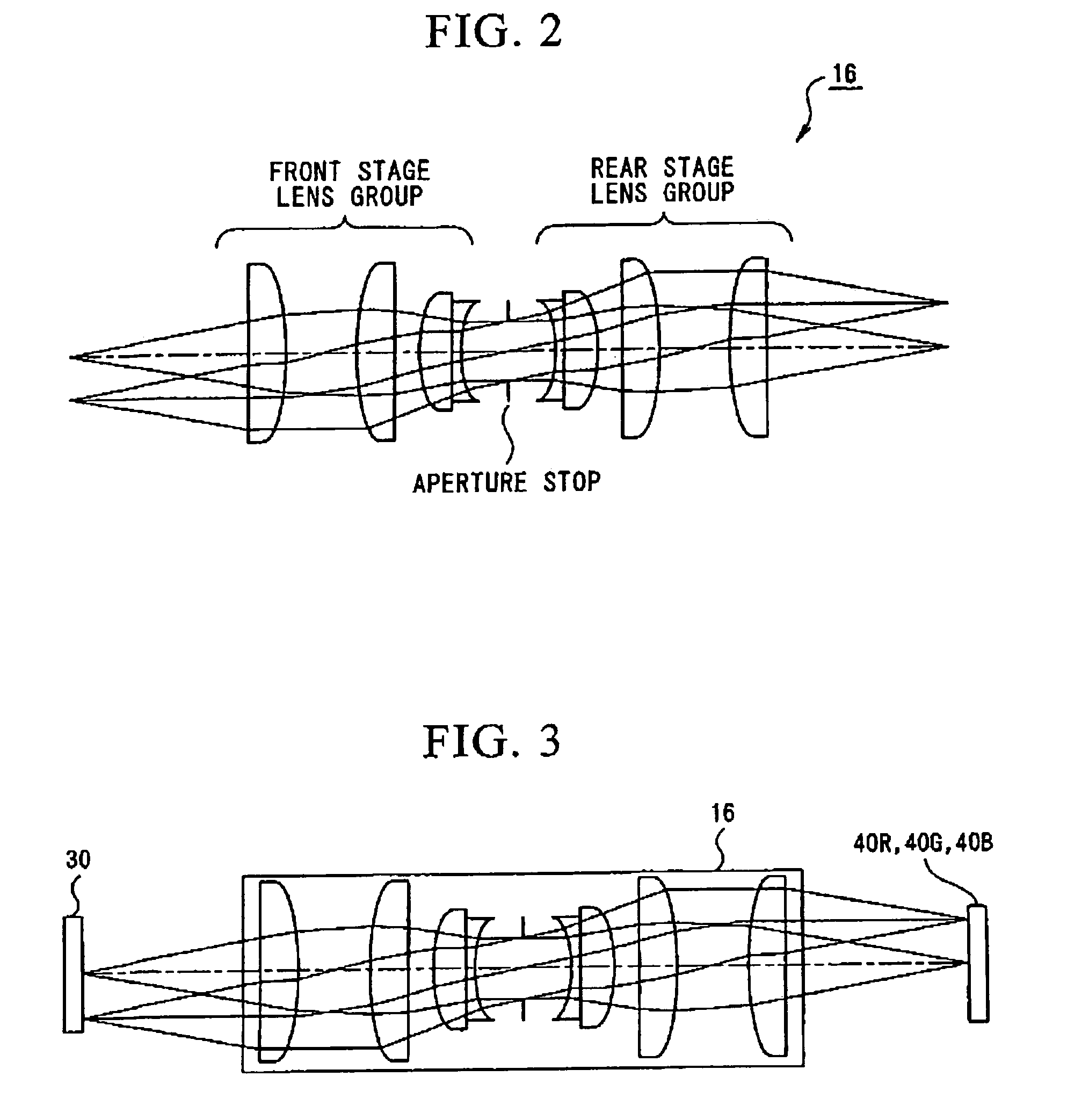
[0090]As shown in FIG. 1, projection-type display 100 is composed of a light source 10, a uniform luminance distribution section 12 that makes the luminance distribution of light en...


PUM

PropertyMeasurementUnit
luminance dynamic rangeaaaaaaaaaa
wavelengthaaaaaaaaaa

Abstract

A projection-type display device 100 including a light source 10, a luminance modulation light valve having a plurality of pixels capable of independently controlling a transmission factor T1, dichroic mirrors 44a and 44b that divided the light from the luminance modulation light valve into the three primary colors of red, green and blue, a plurality of color modulation light valves into which light divided with dichroic mirrors 44a and 44b respectively enters and have a plurality of pixels capable of independently controlling a transmission factor T2, and a dichroic prism 48 that synthesizes light from each of the color modulation light valves, and is provided with a relay optical system 16 on the light path of a luminance modulation section 14 and a color modulation section 18 that forms an optical image of the luminance modulation light valve on the pixel surfaces of each of the color modulation light valves.

Description

BACKGROUND OF THE INVENTION[0001]1. Field of the Invention[0002]The present invention relates to a structure and device as well as a method applied to an optical system that modulates light from a light source through a plurality of optical modulation elements, and more particularly, to an optical propagation structure and optical display device of an optical system preferable for improving imaging accuracy and highly accurate modulation, a light propagation method of an optical system and a display method of an optical display device.[0003]Priority is claimed on Japanese Patent Application No. 2003-427208 filed Dec. 24, 2003, and Japanese Patent Application No. 2004-299284 filed Oct. 13, 2004, the content of which are incorporated herein by reference.[0004]2. Description of the Related Art[0005]Dramatic improvements have been made in recent years in the image quality of liquid cry displays (LCD), EL, plasma displays, cathode ray tubes (CRT), projectors and other optical display dev...

Claims


Application Information

Patent Timeline
Patent Type & Authority Patents(United States)
IPC IPC(8): G03B21/14G02F1/1335G02F1/13G02B27/18G02F1/01G03B21/00H04N5/74H04N9/31
CPCH04N9/315H04N9/3197G03B21/005G03B21/26G03B33/08G03B33/14H04N9/3126
Inventor UCHIYAMA, SHOICHIITOH, YOSHITAKANAKAMURA, JUNICHINITTA, TAKASHIASAHI, TSUNEMORI
Owner SEIKO EPSON CORP
Why Eureka
Try Eureka