Stack type semiconductor apparatus package and manufacturing method thereof

a technology of semiconductor apparatus and manufacturing method, which is applied in the direction of semiconductor devices, semiconductor/solid-state device details, electronic circuit testing, etc., can solve the problems of inability to prepare circuit substrates, requires relatively much work and cost, and cannot solve wire bonding, etc., to achieve convenient manufacturing and inexpensive cost

Active Publication Date: 2007-07-03
SHARP KK
View PDF6 Cites 32 Cited by
  • Summary
  • Abstract
  • Description
  • Claims
  • Application Information

AI Technical Summary

Benefits of technology

[0016]The present invention is made to provide a stack type semiconductor apparatus package which uses a plurality of types of semiconductor apparatus, and which can be easily manufactured with inexpensive cost.
[0018]Unlike the conventional stack type semiconductor apparatus package, the structure provides the following beneficial effect in the case of manufacturing a plurality of types of stack type semiconductor apparatus package including second semiconductor apparatuses having different structures (e.g., the positions of the second electrodes).
[0019]That is, another first circuit substrate does not need to be prepared. Specifically, a first circuit substrate prepared for manufacture of a stack type semiconductor apparatus package including a semiconductor apparatus package is also used for manufacture of another stack type semiconductor apparatus including a different type of second semiconductor apparatus. Such a beneficial effect is obtained by preparing a semiconductor apparatus package (i) whose terminal positions (positions of the first external input / output terminals) are identical to the terminal positions of the semiconductor apparatus package used for the manufacture of the foregoing stack type semiconductor apparatus, and (ii) which includes a second semiconductor apparatus whose type is different from that of the foregoing semiconductor apparatus package. For the preparation of such a semiconductor apparatus package having the identical terminal positions and the different type of second semiconductor apparatus, another second circuit substrate possibly needs to be prepared so as to accommodate to the different type of second semiconductor apparatus. However, the second circuit substrate has a simpler structure than the first circuit substrate does, so that the work and the cost each required for the preparation of the second circuit substrate are less as compared with the work and the cost each required for the preparation of another first circuit substrate. Therefore, only relatively little work and small cost are required for the manufacture of the stack type semiconductor apparatus packages including different types of second semiconductor apparatuses (e.g., semiconductor apparatuses supplied from different semiconductor apparatus manufacturers; and memory semiconductor apparatuses having different memory capacities).
[0021]In the structure, the semiconductor apparatus package is subjected to a test after packaging, irrespective of whether or not the semiconductor apparatus package is a general one. With this, the second semiconductor apparatus provided in the semiconductor apparatus package is substantially guaranteed as the KGD. Therefore, such a second semiconductor apparatus having no defect never causes the stack type semiconductor apparatus package to be entirely defective. In other words, the stack type semiconductor apparatus package never becomes defective as long as the first semiconductor apparatus is a good one. As such, the manufactured stack type semiconductor apparatus package never becomes defective when the first semiconductor apparatus is a good one, so that such a good first semiconductor apparatus is never wasted. Especially, in cases where the second semiconductor apparatus is a memory type semiconductor apparatus (memory element) in a package and the first semiconductor apparatus is a logic type semiconductor apparatus (logic element), the packaging of the second semiconductor apparatus allows the memory type semiconductor apparatus in the package to be substantially guaranteed as the KGD. So, such a memory type semiconductor apparatus having no defect never causes the manufactured stack type semiconductor apparatus package (SiP (system in Package)) to be entirely defective, when the logic type semiconductor apparatus is a good one. Accordingly, such a good and expensive logic type semiconductor is never wasted. As such, the present invention is especially effective in cases where the first semiconductor apparatus is relatively expensive one such as a logical element, and where the second semiconductor apparatus is relatively inexpensive one such as a memory element.
[0024]As described above, the present invention makes it possible that: a first circuit substrate prepared for manufacture of a stack type semiconductor apparatus package, obtained by stacking a semiconductor apparatus package and a semiconductor apparatus on the first circuit substrate, is used for manufacture of another stack type semiconductor apparatus package including a different type of second semiconductor apparatus. With this, another first circuit substrate does not need to be manufactured. As such, with relatively little work and small cost, the present invention makes it possible to provide (i) the stack type semiconductor apparatus packages including different types of second semiconductor apparatuses (e.g., semiconductor apparatuses supplied from different semiconductor apparatus manufacturers; and memory semiconductor apparatuses having different memory capacities), and (ii) the manufacturing method thereof.

Problems solved by technology

Generally, electrode positions (positions of electrodes) are different among various types of semiconductor apparatus, so that the following inconvenience occurs when manufacturing a plurality of such stack type semiconductor apparatus packages having different types of first semiconductor apparatus.
That is, such a difference in the electrode positions makes it impossible that a circuit substrate prepared for a stack type semiconductor apparatus package is used for manufacture of another stack type semiconductor apparatus package having a different type of first semiconductor apparatus (semiconductor apparatus mounted on the circuit substrate in accordance with the flip chip mounting technology), so that another circuit substrate needs to be prepared so as to accommodate to the electrode positions of the semiconductor apparatus having the different type of first semiconductor apparatus.
This requires relatively much work and cost.
However, only wire bonding cannot deal with such a case where the number of the pads and the positions of the pads are different between the memory semiconductor apparatuses.
In the case where the first semiconductor apparatus is not a KGD, a defect of the first semiconductor apparatus possibly causes the stack type semiconductor apparatus package to be entirely defective.

Method used


Image

  • Stack type semiconductor apparatus package and manufacturing method thereof
  • Stack type semiconductor apparatus package and manufacturing method thereof
  • Stack type semiconductor apparatus package and manufacturing method thereof

Examples


embodiment 2

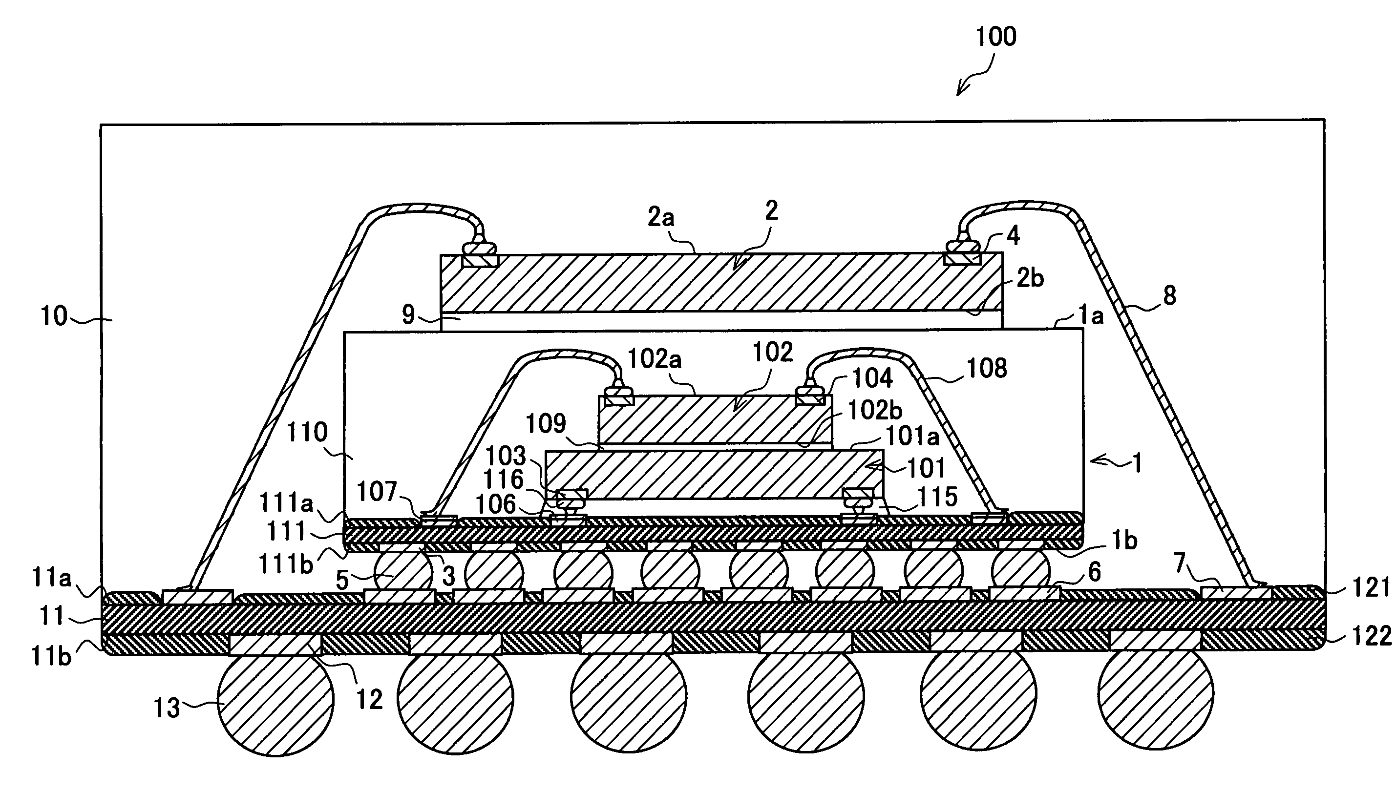
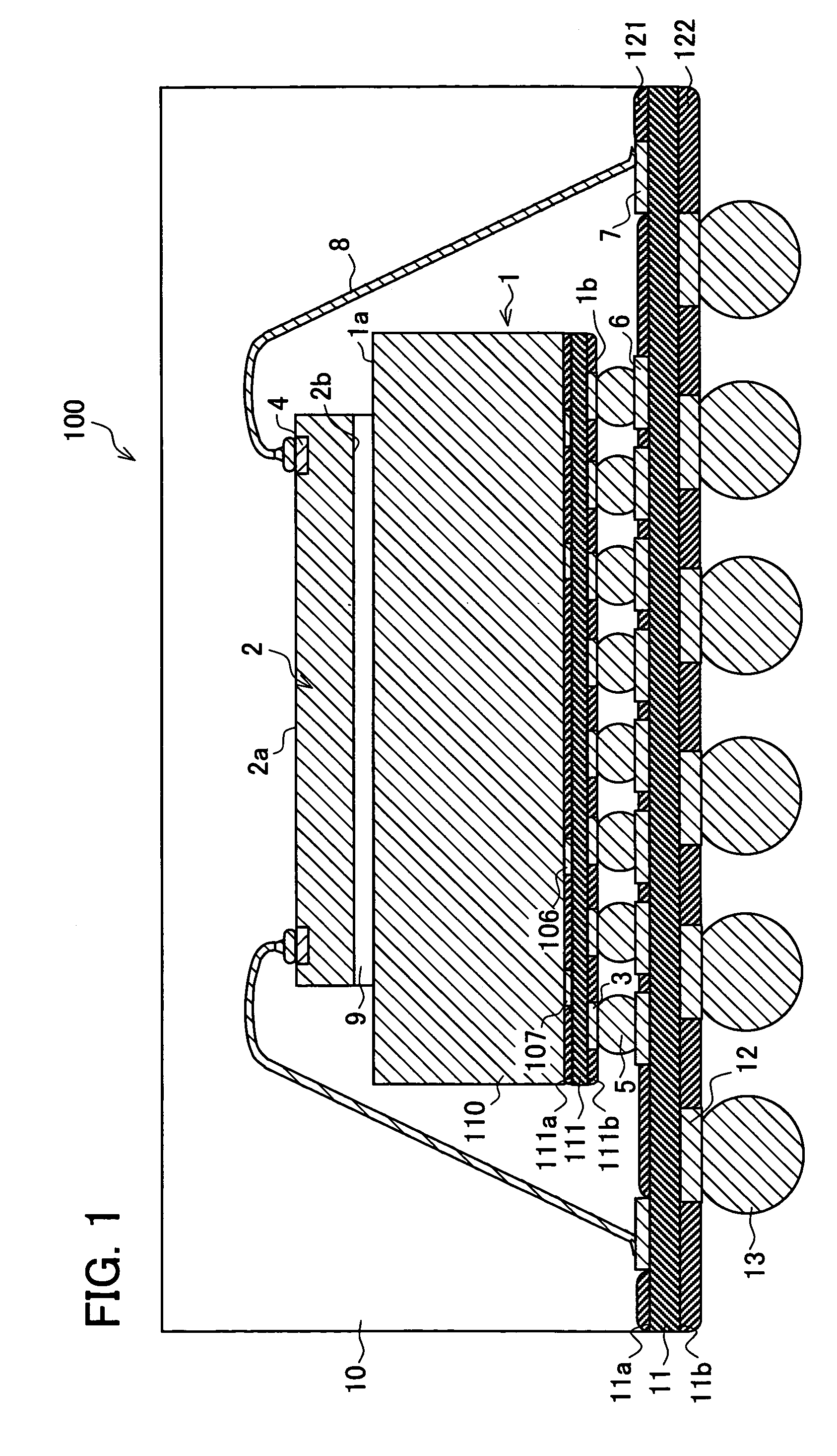
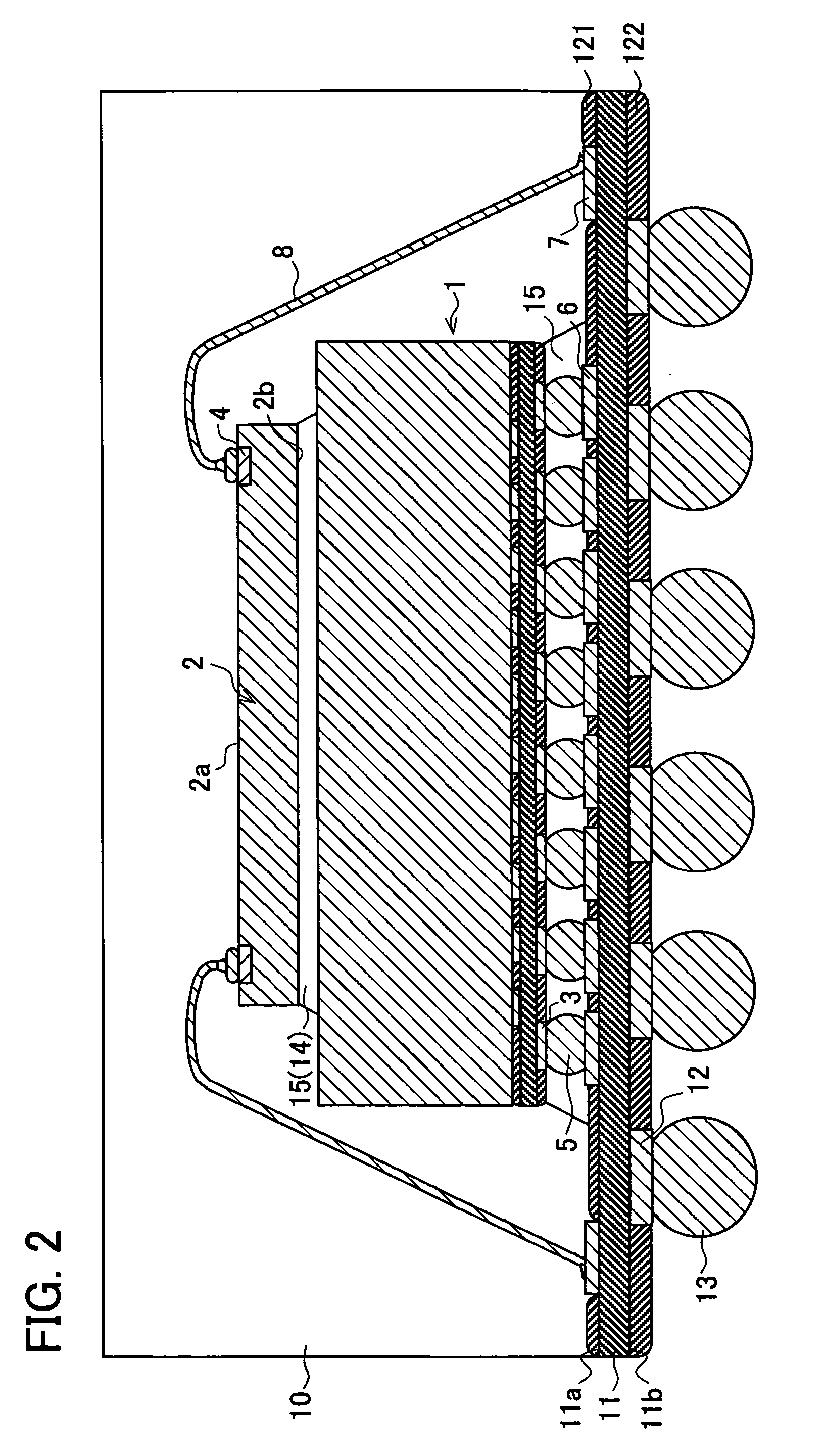
[0109]The following description deals with (i) a stack type semiconductor apparatus package according to another embodiment of the present invention, and (ii) a manufacturing method thereof with reference to FIG. 2, and FIG. 10 to FIG. 20. For ease of explanation, materials having the equivalent functions as those shown in the drawings pertaining to the foregoing Embodiment 1 will be given the same reference symbols, and explanation thereof will be omitted here.

[0110]FIG. 2 is a cross sectional view illustrating the stack type semiconductor apparatus package according to the present embodiment. As shown in FIG. 2, the stack type semiconductor apparatus package according to the present embodiment have the same structure as the structure of the stack type semiconductor apparatus package 100 according to Embodiment 1, except that: (1) instead of the adhesive sheet 9, a liquid resin (liquid adhesive material, adhesive material, third resin) 15 is provided as the adhesive material for ad...

embodiment 3

[0125]The following description deals with (i) a stack type semiconductor apparatus package according to still another embodiment of the present invention, and (ii) a manufacturing method thereof with reference to FIG. 3, FIG. 10, FIG. 11, and FIG. 21 to FIG. 26. For ease of explanation, materials having the equivalent functions as those shown in the drawings pertaining to the foregoing Embodiment 1 or 2 will be given the same reference symbols, and explanation thereof will be omitted here.

[0126]FIG. 3 is a cross sectional view illustrating the stack type semiconductor apparatus package according to the present embodiment. As shown in FIG. 3, the stack type semiconductor apparatus package according to the present embodiment have the same structure as the structure of the stack type semiconductor apparatus package according to Embodiment 2, except that: (1) projection electrodes 16 are provided instead of the projection electrodes 5 that are the solder balls; (2) instead of the cured...

embodiment 4

[0137]The following description deals with (i) a stack type semiconductor apparatus package according to yet another embodiment of the present invention, and (ii) a manufacturing method thereof with reference to FIG. 10 to FIG. 15, and FIG. 27 to FIG. 32. For ease of explanation, materials having the equivalent functions as those shown in the drawings pertaining to any of the foregoing Embodiments 1 to 3 will be given the same reference symbols, and explanation thereof will be omitted here.

[0138]FIG. 32 is a cross sectional view illustrating the stack type semiconductor apparatus package according to the present embodiment. As shown in FIG. 32, the stack type semiconductor apparatus package according to the present embodiment have the same structure as the structure of the stack type semiconductor apparatus package according to Embodiment 2, except that: (1) the internal semiconductor apparatus package 1E is provided instead of the internal semiconductor apparatus package 1D; and (2...


PUM


Abstract

A stack type semiconductor apparatus package includes: (i) a first circuit substrate, (ii) a semiconductor apparatus package mounted on the first circuit substrate, (iii) a semiconductor apparatus, and (iv) a sealing resin for covering them. The first circuit substrate has a surface on which first connecting pads and second connecting pads are provided. The first connecting pads are connected to first external input / output terminals of the semiconductor apparatus package, and the second connecting pads are connected to electrodes of the first semiconductor apparatus, respectively. On a rear surface of the first circuit substrate, there are provided second external input / output terminals connected to the first connecting pads and the second connecting pads. The semiconductor apparatus package includes: a second circuit substrate, and a second semiconductor apparatus mounted on the second circuit substrate. On a surface of the second circuit substrate, there are provided third connecting pads connected to electrodes of the second semiconductor apparatus, respectively. The first external input / output terminals are provided on a rear surface of the second circuit substrate. This makes it possible to provide a stack type semiconductor apparatus package that can be easily manufactured with inexpensive cost.

Description

[0001]This Nonprovisional application claims priority under 35 U.S.C. § 119(a) on Patent Application No. 2004 / 228402 filed in Japan on Aug. 4, 2004, the entire contents of which are hereby incorporated by reference.FIELD OF THE INVENTION[0002]The present invention relates to (i) a stack type semiconductor apparatus package which is used as a CSP (Chip Size Package), a BGA (Ball Grid Array), or the like and which is obtained by stacking a plurality of semiconductor apparatuses; and (ii) a manufacturing method thereof.BACKGROUND OF THE INVENTION[0003]Conventionally used is a semiconductor apparatus package containing a semiconductor apparatus (semiconductor chip).[0004]Downsizing and weight saving of a mobile information device requires high density packaging of semiconductor apparatuses. Proposed in recent years in response to such a demand is a stack type semiconductor apparatus package (stack type multi-chip package) obtained by stacking a plurality of semiconductor apparatuses (se...

Claims


Application Information

Patent Timeline
Patent Type & Authority Patents(United States)
IPC IPC(8): G01R31/28H01L23/02
CPCH01L25/03H01L25/0657H01L25/0652H01L2224/73253H01L2224/32145H01L2224/48091H01L2224/48137H01L2224/48227H01L2224/48465H01L2224/48475H01L2224/73204H01L2224/73265H01L2224/85051H01L2225/0651H01L2225/06517H01L2225/06558H01L2225/06586H01L2924/01078H01L2924/01079H01L2924/14H01L2924/1433H01L2924/15153H01L2924/1517H01L2924/15311H01L2224/16225H01L2924/07811H01L2224/45144H01L2224/32225H01L2924/01019H01L2924/00014H01L2924/00H01L2924/00012H01L24/73H01L2224/0557H01L2224/05573H01L2224/05571H01L2224/0554H01L2224/05599H01L2224/0555H01L2224/0556
Inventor TAMAKI, KAZUO
Owner SHARP KK
Why Eureka
Try Eureka