Thin film magnetic head and manufacturing method thereof
- Summary
- Abstract
- Description
- Claims
- Application Information
AI Technical Summary
Benefits of technology
Problems solved by technology
Method used
Image


Examples
embodiment 1
(1) Embodiment 1
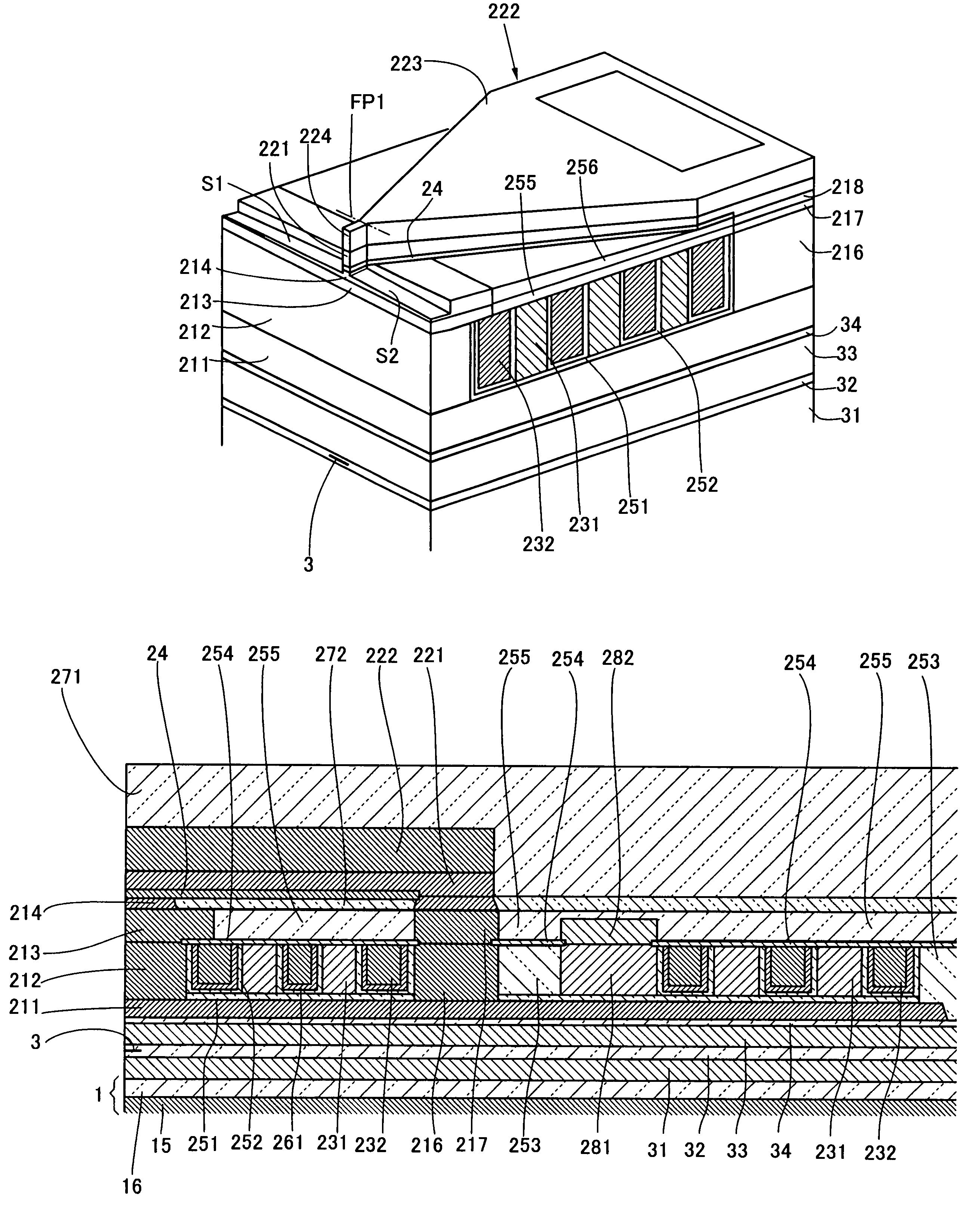
[0149]Embodiment 1 relating to a manufacturing method is a method for manufacturing a thin film magnetic head of a first aspect having a first coil 231 and a second coil 232 (FIGS. 1 to 6). It is notified in advance that processes illustrated in FIGS. 13 to 29 are performed on a wafer.
13>
[0150]Referring to FIG. 13, on an insulating film 16 deposited on a base body 15 there are formed a first shield film 31, a read element 3, an insulating film 32, a second shield film 33, an insulating film 34 and a first magnetic film 211 by means of publicly known processes.
[0151]In a specific example, the insulating film 16 is an alumina film, formed, for example, 3 μm in thickness. The first shield film 31 is made of a magnetic material such as NiFe and formed 2 to 3 μm in thickness by a frame-plating method. The insulating film 32 is, in general, formed by the following two steps: in the first step, an alumina film of 3 to 4 μm in thickness is formed, and then the surface of the...
embodiment 2
(2) Embodiment 2
[0191]Embodiment 2 relates to a method for manufacturing a thin film magnetic head shown in FIGS. 7 and 8. FIGS. 30 to 38 show processes of this manufacturing method. It is notified in advance that processes illustrated in FIGS. 30 to 38 are also performed on a wafer.
30>
[0192]In the process leading to the state of FIG. 30, processes illustrated in FIGS. 13 to 19 of embodiment 1 are performed to obtain substantially the same structure as in FIG. 19, and then the following processes are performed.
[0193]First, an insulating film 254 covering the surfaces of the first coil 231 and the second coil 232 is deposited thereon. The insulating film 254 is made of Al2O3 and formed, for example, 0.2 to 0.3 μm in thickness.
[0194]Next, a photolithography process is performed on one surface where the insulating film 254 has been formed, so that a resist frame for forming a connecting conductor 282 for connecting the inner end 281 of the first coil 231 with the outer end 283 of the s...
embodiment 3
(3) Embodiment 3
[0219]Embodiment 3 is a manufacturing process for a thin film magnetic head shown in FIGS. 9 and 10, and is illustrated in FIGS. 39 to 47. Processes, which have been illustrated and described in embodiment 1 or 2 and are also applied to embodiment 3, are referred to the description of embodiment 1 or 2 and the illustrations of the processes may be omitted.
39>
[0220]In the process leading to the state of FIG. 39, processes illustrated in FIGS. 13 to 15 of embodiment 1 are performed to obtain substantially the same structure as in FIG. 15, and then the following processes are performed.
[0221]First, the photoresist film RS2 is removed and then, an insulating film 252 of about 0.1 to 0.15 μm in thickness is deposited on the surfaces and side surfaces of the insulating film 251, the first coil 231, the second pole piece 212 and the back gap piece 216. In case of forming the insulating film 252 as an Al2O3 film, it is possible to adopt an alumina-CVD film forming method in ...
PUM
| Property | Measurement | Unit |
|---|---|---|
| Width | aaaaa | aaaaa |
| Depth | aaaaa | aaaaa |
| Height | aaaaa | aaaaa |
Abstract
Description
Claims
Application Information