NAND-structured flash memory

a flash memory and structure technology, applied in the field of nonvolatile semiconductor memory devices, can solve the problems of erroneous writing, low performance, and complex control circuits,

Active Publication Date: 2007-07-03
KIOXIA CORP
View PDF7 Cites 88 Cited by
  • Summary
  • Abstract
  • Description
  • Claims
  • Application Information

AI Technical Summary

Problems solved by technology

If the writing characteristics are different in the memory cell at the end of the NAND string such as the memory cell next to the selection gate, and the memory cell in the center of the NAND string, it is necessary to individually control the voltage applied to a control gate of the memory cell, for example, depending on where the selected cell is located, and thus a complicated control circuit is needed to achieve this.
However, if the writing characteristics are significantly different in the memory cells, more time is spent in the step-up writing to reduce the width of threshold distribution, leading to lower performance.
In this way, “erroneous writing” occurs where a charge is injected into the floating gate of the selected cell whose state should not be changed.
Furthermore, parasitic capacitance and resistance increase along with the increase in the length of the word line and bit line, which is a disadvantage to the performance of a chip, and therefore, some measures need to be taken.
For example, the increased bit line length poses such problems that the pre-charge time is increased, that time is increased for a cell current to cause a small potential difference in the bit line, and that time is increased for the bit lines to recover their original state.
Moreover, the following problems are posed in a reading operation of the NAND-structured flash memory.
In this case, however, in the conventional structure of the NAND string, when the cell linked to the non-selected bit line serving as a shield has a negative threshold value (“1”), opening the selection gate will cause the current to flow from its bit line to the source line to lower the potential, resulting in a problem that it cannot serve as the shielding line.

Method used


Image

  • NAND-structured flash memory
  • NAND-structured flash memory
  • NAND-structured flash memory

Examples


first embodiment

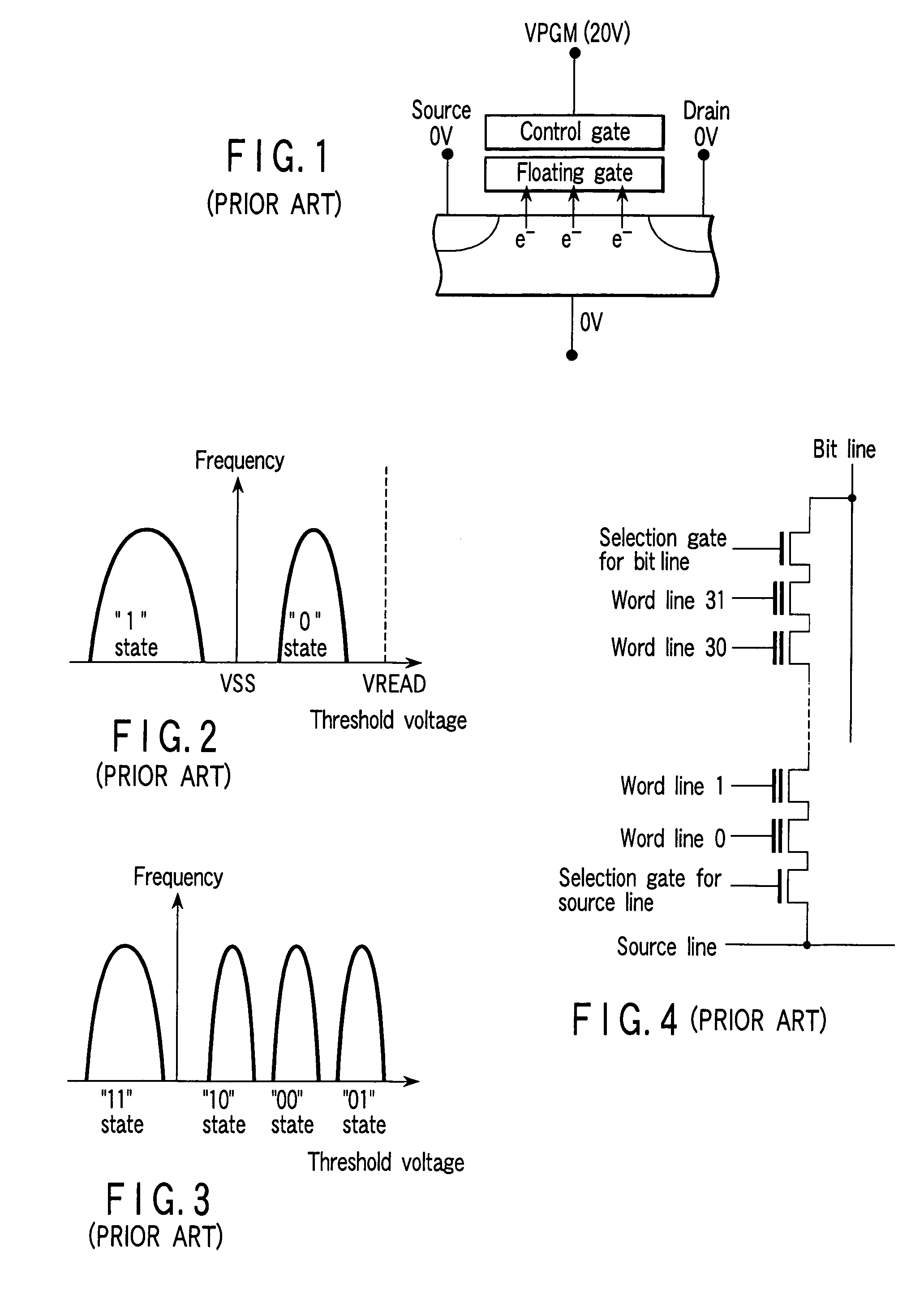
[0064]Before describing the embodiments, a bias condition in writing into a NAND-structured flash memory is shown in FIG. 1 to reconfirm characteristics of the NAND-structured flash memory. In this method, a channel is fixed at ground potential, and a high potential (hereinafter referred to as VPGM) is applied to a control gate which is a word line, so as to pull electrons from the entire channel, and store the electrons in a floating gate. A threshold value of a memory cell transistor changes in accordance with the amount of electric charge stored in the floating gate.

[0065]As shown in FIG. 2, in a NAND structure using a binary cell, a state in which electrons are stored in the floating gate and a state in which electrons are not stored are identified to store one bit. Further, as shown in FIG. 3, in a NAND structure using a multi-level cell, the threshold value of the memory transistor which changes in accordance with the amount of electric charge stored in the floating gate is id...

second embodiment

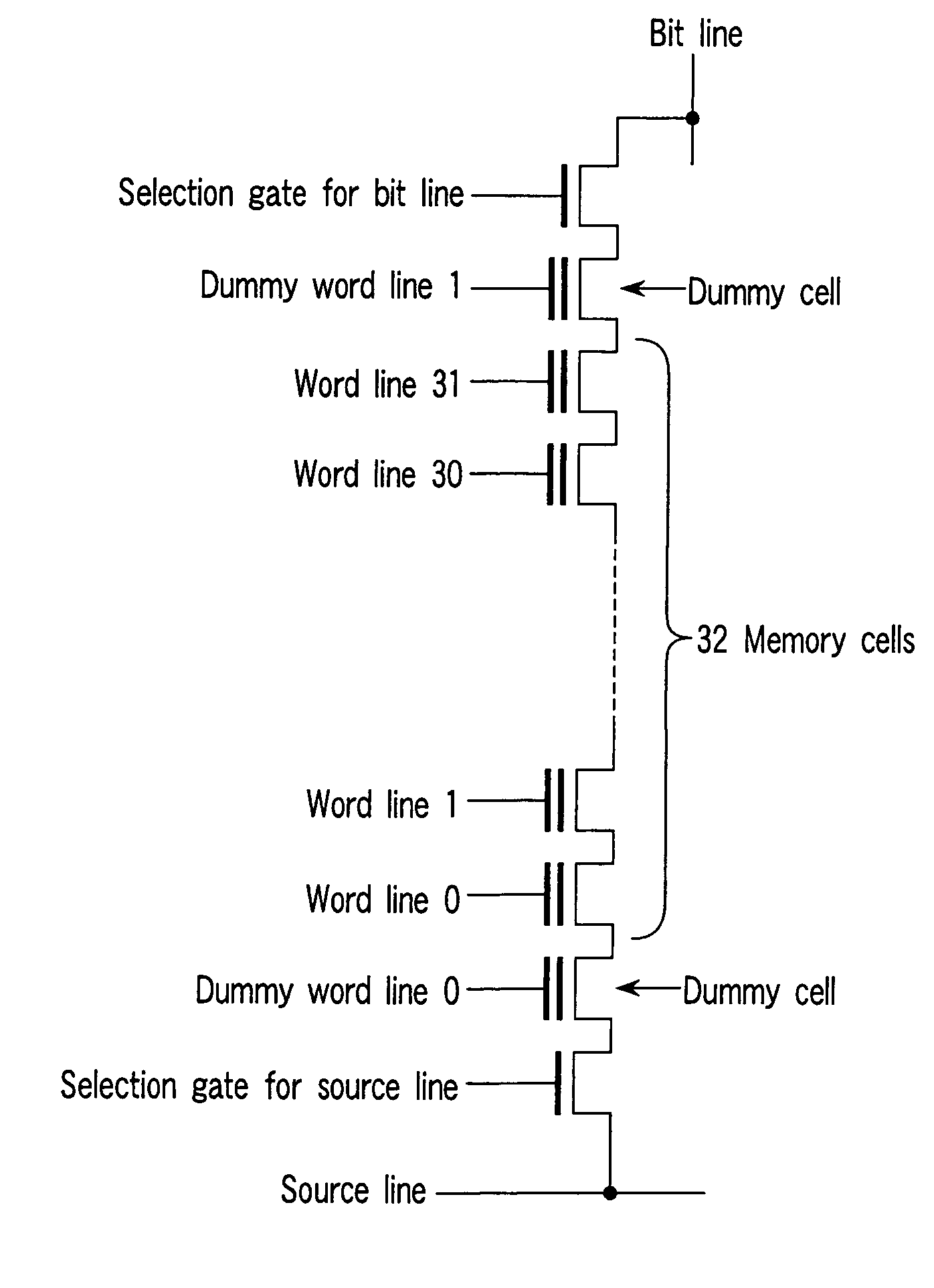
[0082]The NAND-structured flash memory in a second embodiment is a quaternary NAND-structured flash memory, and as shown in FIG. 11, one NAND string is composed of the bit line side selection gate (selection transistor), 36 memory cells, and the source line side selection gate. The four memory cells including two next to the bit line side selection gate and two next to the source line side selection gate are treated as dummy cells (dummy gates), and the remaining 32 memory cells are treated as quaternary cells. As the two dummy cells are disposed next to the selection gate, it is possible to have a more uniform bias condition in the operation of writing into the quaternary cells than in the first embodiment.

[0083]The circuit in FIG. 10 of the first embodiment can be utilized directly as a word line voltage control circuit. In addition, a quaternary memory cell is also used for the dummy cell in the second embodiment, but a memory cell higher than the quaternary level such as the oct...

third embodiment

[0084]The NAND string in a third embodiment has the same configuration as that in the second embodiment, but a control gate charging voltage for the dummy cells adjacent to the selection gates is lower (e.g., 2.5 V) than the ordinary non-selected word line voltage (e.g., 14 V). This makes it possible to keep the effects of the coupling noise lower, which are caused to the selection gate when the control gate is charged.

[0085]FIG. 12 is a circuit diagram of the word line voltage control circuit (word line driving circuit) capable of the operation described above. The difference from the word line voltage control circuit in FIG. 10 is that a first dummy word line voltage generator 6, a second dummy word line voltage generator 7, a first dummy word line voltage selection circuit 8 and a second dummy word line voltage selection circuit 9 are added. As two dummy word line voltage generators are provided, the bit line side dummy gate and the source line side dummy gate can be driven at di...


PUM


Abstract

A NAND-structured flash memory comprises a memory cell array wherein plural memory strings are arranged in matrix form, each of the memory cell strings including plural nonvolatile memory cells, the first conducting paths of the memory cells being connected in series, at least one of the memory cells having a function other than an external data storing function, plural first selection transistors having second conducting paths, and one end of the second conducting paths being connected to one end of the series of the first conducting paths, respectively, plural bit lines connected to the other end of the second conducting paths, plural second selection transistors having third conducting paths, and one end of the third conducting paths being connected to one end of the series of the first conducting paths, respectively, and a source line connected to the other end of the third conducting paths.

Description

CROSS-REFERENCE TO RELATED APPLICATIONS[0001]This application is based upon and claims the benefit of priority from prior Japanese Patent Application No. 2004-040132, filed Feb. 17, 2004, the entire contents of which are incorporated herein by reference.BACKGROUND OF THE INVENTION[0002]1. Field of the Invention[0003]The present invention relates to a nonvolatile semiconductor memory device, especially a NAND-structured flash memory, and in particular relates to a configuration of a core portion of the memory and its control circuit.[0004]2. Description of the Related Art[0005]Recently, an EEPROM (NAND-structured flash memory) having NAND-structured cells has often been used as an EEPROM having a larger capacity in digital devices such as digital cameras and mobile telephones.[0006]Various improvements have been attempted in the NAND-structured flash memory with increasing use thereof. For example, in Jpn. Pat. Appln. KOKAI Publication No. 10-199280, driving is performed with a pair ...

Claims


Application Information

Patent Timeline
Patent Type & Authority Patents(United States)
IPC IPC(8): G11C11/34G11C16/02G11C16/04G11C16/06
CPCG11C11/5621G11C16/0483G11C2211/5641
Inventor ABE, TAKUMIMAEJIMA, HIROSHIFUKUDA, KOICHIHARA, TAKAHIKO
Owner KIOXIA CORP
Why Eureka
Try Eureka