Optical waveguide termination with vertical and horizontal mode shaping

a technology of optical waveguides and waveguides, applied in the direction of optical radiation measurement, instruments, spectrometry/spectrophotometry/monochromators, etc., can solve the problems of limited density per wafer in optical integrated circuits, inability to directly coupling high delta-n waveguides to commonly used single-mode optical, and inability to achieve high delta-n waveguides

Inactive Publication Date: 2007-07-31
SAMSUNG ELECTRONICS CO LTD
View PDF77 Cites 45 Cited by
  • Summary
  • Abstract
  • Description
  • Claims
  • Application Information

AI Technical Summary

Problems solved by technology

Although the technology is maturing rapidly, optical integrated circuits are still an order of magnitude larger than their electrical counterparts because of the large bend radius, large core size, and limited mode confinement of current, “low delta-n” (low refractive index differential) planar optical circuits.
However, only limited density per wafer can be achieved in such OICs.
Despite such potential benefits, high delta-n waveguides yet remain to be adopted due to a number of challenges.
One of the greatest challenges preventing the commercial use of high delta-n waveguides is that high delta-n waveguides are not well suited for direct coupling to commonly used single mode optical fiber that typically has a 7 μm to 9 μm mode field diameter.
Therefore, a challenge is to provide a waveguide transition region that enables adiabatic expansion of the mode so that it is supported by the optical fiber.
Fabricating a waveguide to effect adiabatic expansion of the mode in the vertical direction has proven difficult using conventional fabrication techniques.
For example, tapering the thickness of the waveguide to effect the vertical adiabatic expansion of the mode is exceedingly difficult by conventional techniques.

Method used


Image

  • Optical waveguide termination with vertical and horizontal mode shaping
  • Optical waveguide termination with vertical and horizontal mode shaping
  • Optical waveguide termination with vertical and horizontal mode shaping

Examples


example i

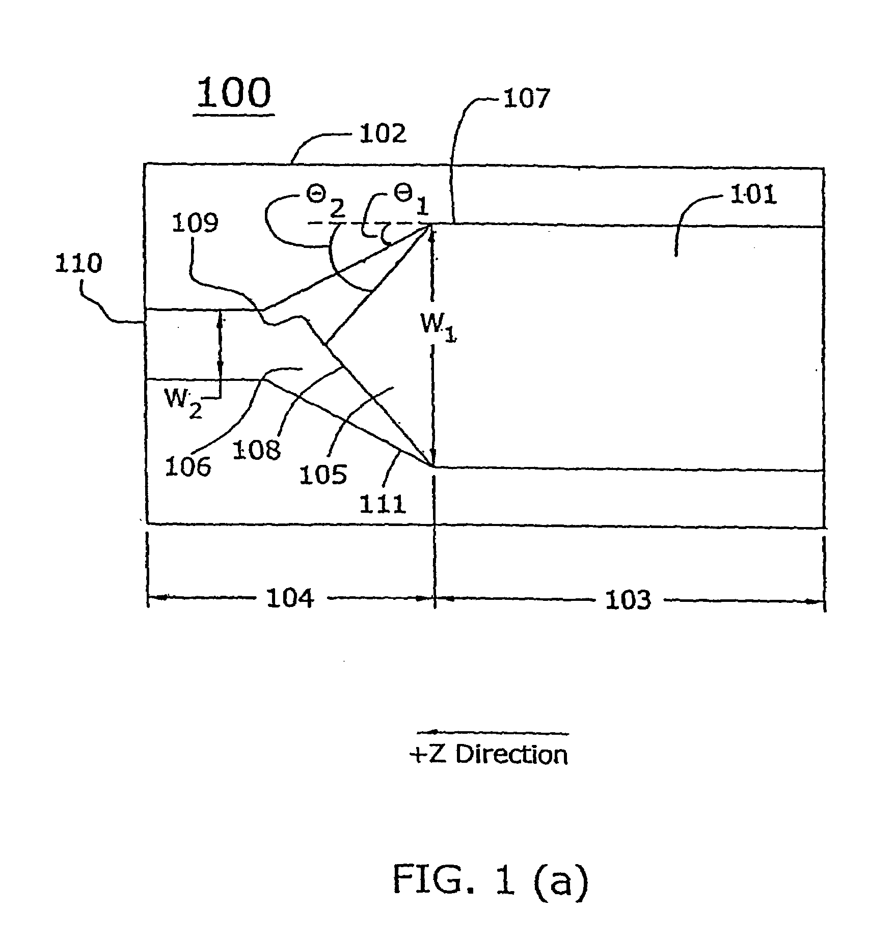
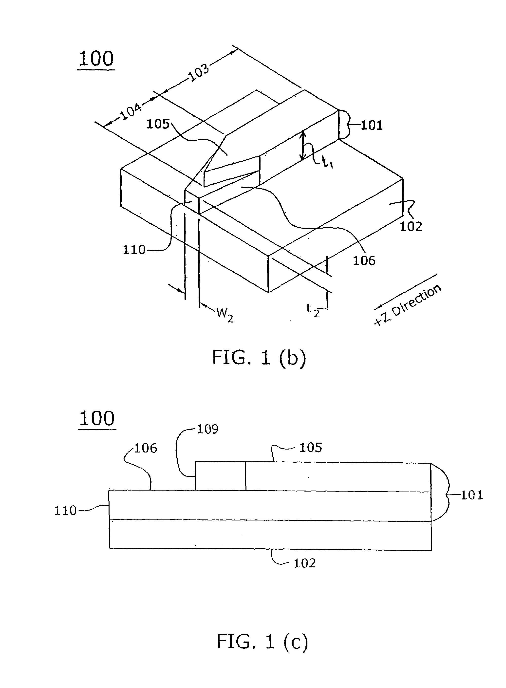
[0040]Turning to FIG. 2(a), a perspective view of a waveguide 200 according to an exemplary embodiment of the present invention is shown. A lower cladding layer 202 is disposed on a substrate 201. A guiding layer 203 is disposed on lower cladding layer 202. Waveguide 200 has a first region 204 and a second region 205. The guiding layer 203 includes a lower portion 206 and an upper portion 207. An optical mode is coupled from an endface 209 to an optical fiber 208. For the purposes of ease of discussion, an upper cladding layer is not shown in FIG. 2(a). This upper cladding layer would cover the guiding layer 203. The upper cladding layer, guiding layer 203 and lower cladding layer 202 form a waveguide 200 according to an illustrative embodiment of the present invention. The upper cladding layer may have the same index of refraction as the lower cladding layer 202. Alternatively, the upper cladding layer may have a higher (or lower) index of refraction as the lower cladding layer 202...

example ii

[0057]As described above, the upper portion 207 and lower portion 206 of the guiding layer 203 in Example I were substantially symmetric about an axis 210 bisecting the guiding layer 203. In the illustrative embodiments of Example II, the upper portion 407 of the guiding layer 401 may be asymmetric about an axis 413 bisecting the guiding layer 401. The lower portion 402 may be symmetric about the axis 413 bisecting the guiding layer 401. Alternatively, both the upper portion 407 and the lower portion 402 may be asymmetric about an axis 413 bisecting the guiding layer 401. The asymmetry of either the upper portion 407 of the guiding layer 401 alone or of the upper and lower portions 407 of the guiding layer 401 about an axis 413 which bisects the guiding layer 401 may be beneficial from the perspective of manufacturing and fabrication.

[0058]In the illustrative embodiments described in this example, the asymmetry of the taper of either the upper portion 407 or the upper portion 407 an...

example iii

[0069]In the present example, other illustrative embodiments of the present invention are described. These illustrative embodiments may incorporate the principles of symmetry and asymmetry of the guiding layer as described above. Moreover, many of the fabrication techniques described in connection with the illustrative embodiments of Examples I and II may be used.

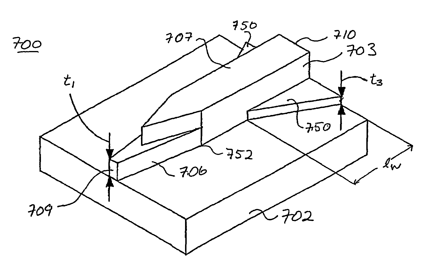
[0070]FIG. 5 shows a perspective view according to another illustrative embodiment of the present invention. A waveguide 500 includes a lower cladding layer 502. The lower cladding layer 502 may be disposed on a substrate 501. A guiding layer 503 is disposed on the lower cladding layer 502. An upper cladding layer (not shown) may be disposed on the guiding layer 503. In the embodiment shown in FIG. 5, the lower portion 507 of the guiding layer 503 is a diffused guiding layer. In the particular embodiment shown in FIG. 5, the lower portion 507 is illustratively a TiLiNbO3 waveguide. The top portion 506 of waveguide 503 is a ...


PUM

PropertyMeasurementUnit
angleaaaaaaaaaa
angleaaaaaaaaaa
thicknessaaaaaaaaaa

Abstract

An optical device is disclosed which includes a single-mode waveguide (700) which supports a first optical mode in a first region and a second optical mode in a second region. The waveguide includes a guiding layer (703) having at least one wing (750) extended outwardly from the guiding layer (703). The guiding layer (703) may desirably have a rib waveguide (706, 707) cross sectional shape at the wings. The wings (750) decrease in width along the length of the guiding layer to convert a rib waveguide mode at the wings to a channel waveguide mode.

Description

RELATED APPLICATIONS[0001]This application is a National Stage of International Application No. PCT / US02 / 38553, filed Dec. 5, 2002, which claims the benefit of priority of U.S. Provisional Application 60 / 336,933, filed on Dec. 5, 2001. This application is also a continuation-in-part application of International Application No. PCT / US01 / 51497, filed on Dec. 14, 2001, which claims the benefit of priority of Provisional Application No. 60 / 255,868, filed Dec. 14, 2000 and Provisional Application No. 60 / 287,032, filed Apr. 30, 2001. The entire contents of the above-referenced application(s) are incorporated herein by reference.FIELD OF THE INVENTION[0002]The present invention relates generally to optical integrated circuits (OIC), and particularly to, a structure for coupling optical waveguides.BACKGROUND OF THE INVENTION[0003]Optical communications are evolving as the chosen technique for data and voice communications. Currently most OICs in the optical network are passive components th...

Claims


Application Information

Patent Timeline
Patent Type & Authority Patents(United States)
IPC IPC(8): G02B6/10C12M1/34G01J3/42G01J3/427
CPCG02B6/1228G02B6/305G02B6/14
Inventor LUO, HUIDAUTARTAS, MINDAUGAS F.STEINBERG, DAN A.SHERRER, DAVID W.
Owner SAMSUNG ELECTRONICS CO LTD
Why Eureka
Try Eureka