

Optical substrate, semiconductor light-emitting element and method of manufacturing semiconductor light-emitting element
a technology of semiconductor light-emitting elements and optical substrates, which is applied in semiconductor/solid-state device testing/measurement, lighting and heating apparatus, instruments, etc., can solve the problems of significant and disadvantageous reduction of light extraction efficiency, and achieve the enhancement improvement of internal quantum efficiency iqe, and improvement of light extraction efficiency lee
- Summary
- Abstract
- Description
- Claims
- Application Information
AI Technical Summary
Benefits of technology
Problems solved by technology
Method used
Image

Examples
example 1
[0658]On a c-plane sapphire substrate having a diameter φ2″ and a thickness of 0.33 mm, a mask material was applied by a spin coating method (2000 rpm, 20 seconds) to form a resist layer. As the mask material, an application solution was used which was diluted by propylene glycol monomethyl ether such that the solid content of a photosensitive resin composition was 5 weight %.
[0659]As the photosensitive resin composition, the followings were mixed and used: 20 weight parts of 3-ethyl-3{[3-ethyloxetan-3-yl)methoxy]methyl}oxetane (OXT-221, made by Toagosei Co., Ltd.); 80 weight parts of 3′,4′-epoxy cyclohexane carboxylic acid-3,4-epoxy cyclohexyl methyl (Wako Pure Chemical Industries, Ltd.); 50 weight parts of phenoxy diethylene glycol acrylate (Aronix (registered trademark) M-101A, made by Toagosei Co., Ltd.); 50 weight parts of ethylene oxide-modified bisphenol A diacrylate (Aronix (registered trademark) M-211B, made by Toagosei Co., Ltd.); 8 weight parts of DTS-102 (made by Midori ...
example 2
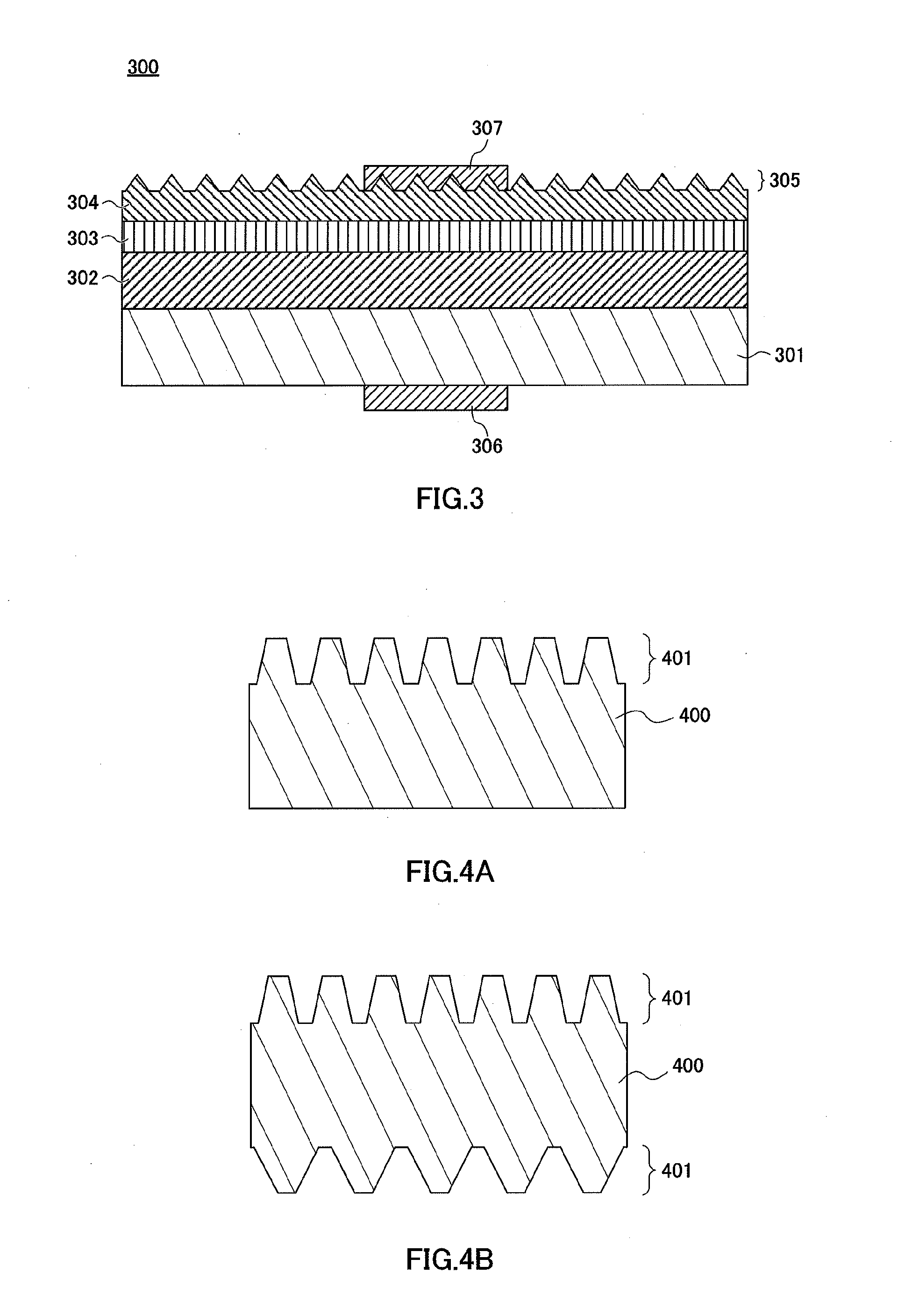
[0670]In the production of the optical substrates (A) to (C) according to example 1, the same operation was performed to produce the sapphire substrates except that the inverted resin molds (1) to (3) were changed to the resin molds (1) to (3). The surface and the cross section of the obtained sapphire substrates were observed with a scanning electron microscope.
[0671]The sapphire substrate (D) produced by using the resin mold (1) had an average concave portion depth Dave of 105 nm and an average interval Pave of 200 nm. The minimum value of the concave portion depth dn was 0 nm because it is estimated that it was the part to which no pulse was applied. For the minimal concave portion corresponding to dn=0 nm, the bottom portion of the minimal concave portion was observed. Since roughness was observed in the bottom portion, the outline of the minimal concave portion was able to be observed to be substantially circular. That is, dn=0 nm does not mean that there is nothing in the part...
example 3
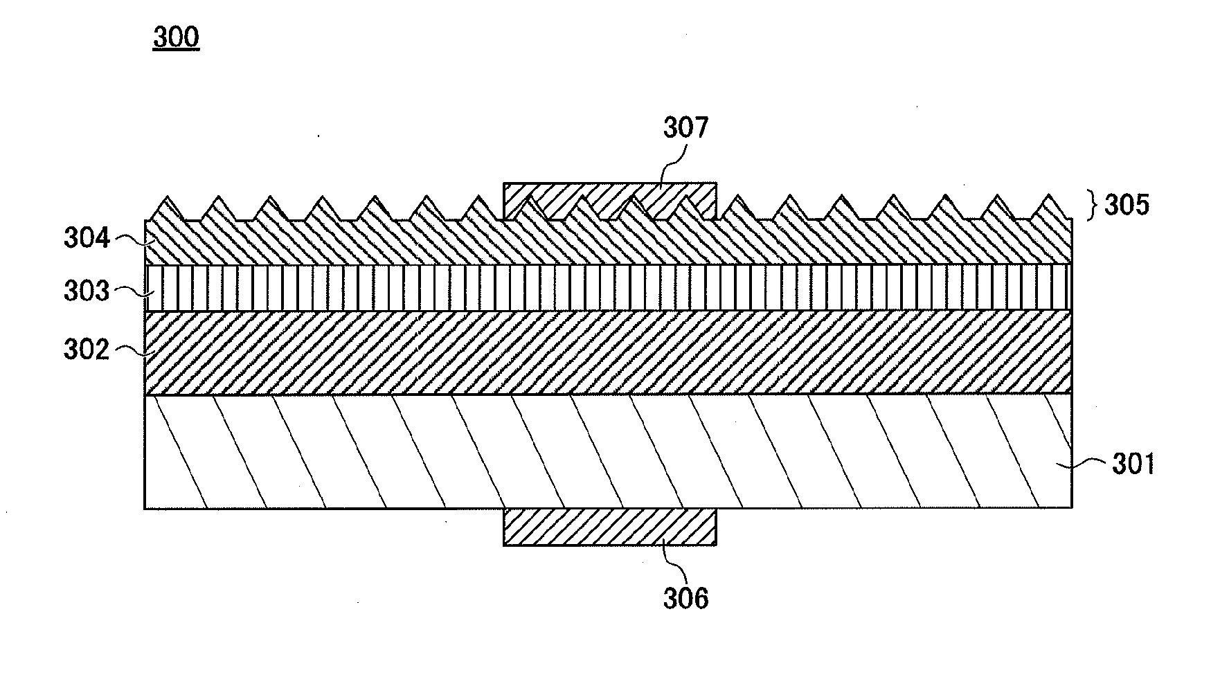
Production of a Semiconductor Light-Emitting Element
[0686]On the sapphire substrates (the optical substrates (A) to (F)) obtained in examples 1 and 2, the followings were continuously deposited by a metal organic chemical vapor deposition method (MOCVD): (1) AlGaN low-temperature buffer layer, (2) n-type GaN layer, (3) n-type AlGaN clad layer, (4) InGaN light-emitting layer (MQW), (5) p-type AlGaN clad layer, (6) p-type GaN layer and (7) ITO layer, and the semiconductor light-emitting element (A) was produced. The concave and convex portions on the sapphire substrate were embedded and flattened under conditions of film formation when the (2) n-type GaN layer was deposited. Then, the semiconductor light-emitting element (A) was etched, and an electrode pad was attached. In this state, a prober was used to pass a current of 20 mA between a p-electrode pad and an n-electrode pad, and the light emission output of the semiconductor light-emitting element (A) was measured. The light emiss...
PUM
 Abstract
Description
Claims
Application Information