Thermal management for shielded circuit packs

a shielded circuit and thermal management technology, applied in the direction of electrical apparatus contruction details, semiconductor/solid-state device details, lighting and heating apparatus, etc., can solve the problems of insufficient conduction through the pcb to keep junction temperature below the maximum operating limit, difficult to achieve cooling using this general technique, and variations in ic stack-up height and parallelism to the pcb. , to achieve the effect of improving thermal management, efficient cooling and low thermal resistan

Inactive Publication Date: 2007-08-07
WSOU INVESTMENTS LLC +1
View PDF8 Cites 35 Cited by
  • Summary
  • Abstract
  • Description
  • Claims
  • Application Information

AI Technical Summary

Benefits of technology

[0007]More particularly, the aspects of the present invention provide a heat transfer device or assembly for EMI shielded circuit packs whereby multiple heat sources (e.g., high-power components) are cooled by an individual heat-dissipating structure (e.g., a heat sink) which protrudes, in part, into an external airflow through individual openings in the lid of the EMI shield. That is, each heat source has its own individual heat sink. Importantly, in accordance with the principles of the invention, mechanically-compliant, electrically-conductive gaskets are used to seal the base plates of the individual heat sinks against the lid of the EMI shield enclosure. As such, in accordance with the various aspects of the invention, the conductive gaskets establish a compliance layer which accommodates any variation in the heights of the individual components, thereby, allowing optimum thermal contact between the components and their respective heat sinks without compromising the EMI shielding. That is, in accordance with the principles of the invention, the mechanically-compliant layer (sometimes alternatively referred to herein as the “compliance layer”) of the heat transfer assembly is external to the thermal path delivered thereby. Significantly, as the compliance layer is not in the thermal path this allows for the application of an optimally thin layer of thermal grease at the interface of the component and its respective heat sink. Further, the gaskets of the invention are mechanically compliant and allow the entire circuit packet assembly to adapt to dimensional variations without adversely affecting the thermal path. Importantly, solid-to-solid contact (e.g., the top of the IC package to the bottom plate of the heat sink) is maintained along the entire IC / heat sink contact area thereby keeping thermal resistance at a very low level.
[0008]Advantageously, the heat transfer device / assembly of the present invention provides a certain adaptability to physical variations in EMI shielded circuit packs (e.g., component gaps, component height variations and misalignment) while improving the thermal management achieved within such circuit packs. Importantly, in accordance with the principles of the invention, the mechanically-compliant layer of the heat transfer assembly is external to the thermal path. Said another way, the mechanically-compliant layer of the heat transfer assembly is physically separated from the thermal path delivered thereby but is integral with the EMI shield. Further, advantageously, efficient cooling is achieved in that the individual heat sinks can be tailored to the thermal load associated with their respective component. Additionally, the set of individual heat sinks, in accordance with the principles of the invention, can present a lower thermal resistance to the cooling airflow than a conventional configuration of fins covering the entire lid of the EMI shield (see, for example, FIG. 1C). Also, improved serviceability of circuit packs is achieved due to the need of only removing the lid (which is not adhered to the rest of the circuit pack by layers of thermal grease or thermally-conductive adhesive) and, if necessary, the heat sinks from components under repair. Thus, the mechanical stresses encountered upon opening the circuit pack for inspection and / or repair are modest, and the circuit pack can remain powered, with appropriate cooling, while under inspection and / or repair.

Problems solved by technology

Circuit packs and modules typically have one or more printed circuit board (PCB)-mounted integrated circuits (ICs) that dissipate enough heat that cooling by simple, un-enhanced natural convection, radiation and / or by heat conduction through the PCB is insufficient to keep junction temperatures below maximum operating limits.
Cooling using this general technique, however, is not always easy to achieve.
For instance, variations in IC stack-up height and parallelism to the PCB present notable problems.
However, air circulated by cooling fans in such products cannot penetrate the EMI shield thereby leading to disastrous results.
For example, due to the high thermal resistance between such components their ambient component temperatures can be too high to achieve the desired product and individual component reliability and performance.
Further, and potentially more damaging, elevated temperatures can destroy the components at certain higher temperature levels.
However, a problem that may be encountered in making a proper thermal connection between the ICs and the heat sink is that the distance between the heat sink and the ICs can vary, both because of IC stack-up height variations and because of thermal expansion of the entire assembly.
As such, it is often difficult to achieve a proper, reliable contact between surfaces to maintain a good thermal path.
Additionally, the two surfaces to be thermally connected may not be sufficiently parallel and in fact may shift relative to one another as the assembly is transported, or thermally or mechanically stressed.
Unfortunately, this results in an undesirably large increase in component temperatures.
Moreover, in practice, the thermal grease is squeezed out of the gap as the components are pressed together, and then, if the gap re-opens up it cannot refill the gap.

Method used


Image

  • Thermal management for shielded circuit packs
  • Thermal management for shielded circuit packs
  • Thermal management for shielded circuit packs

Examples


Embodiment Construction

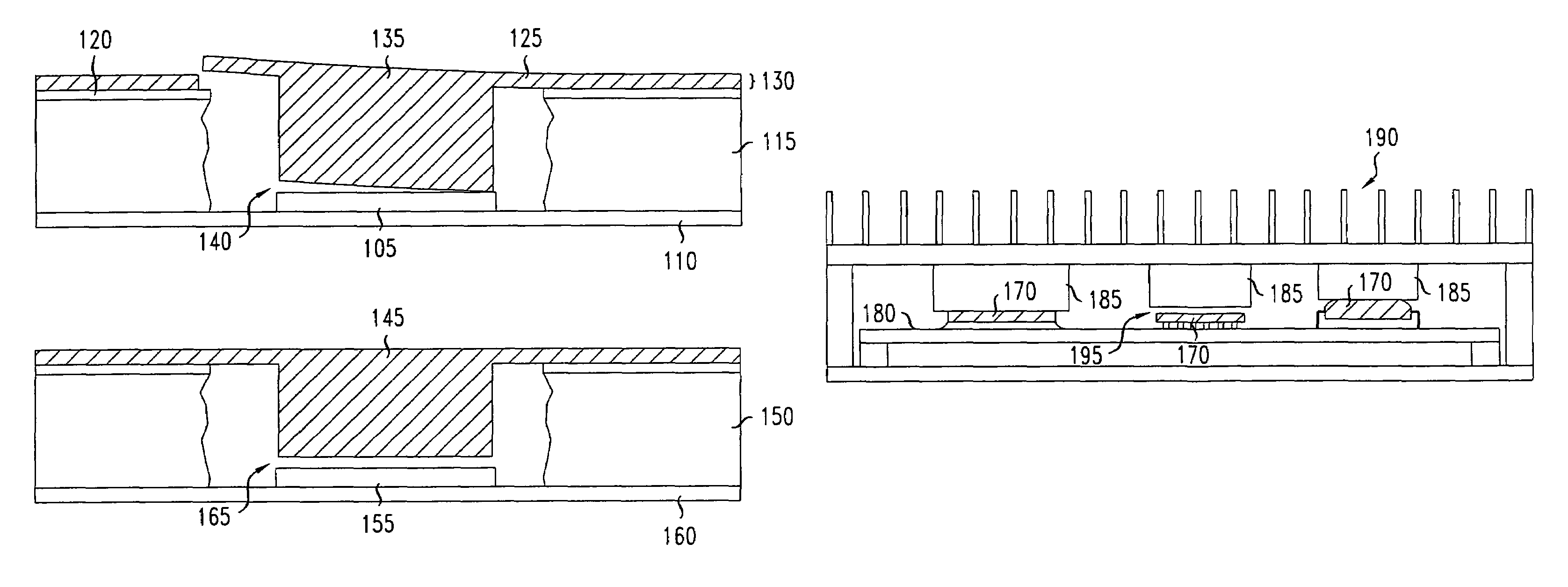
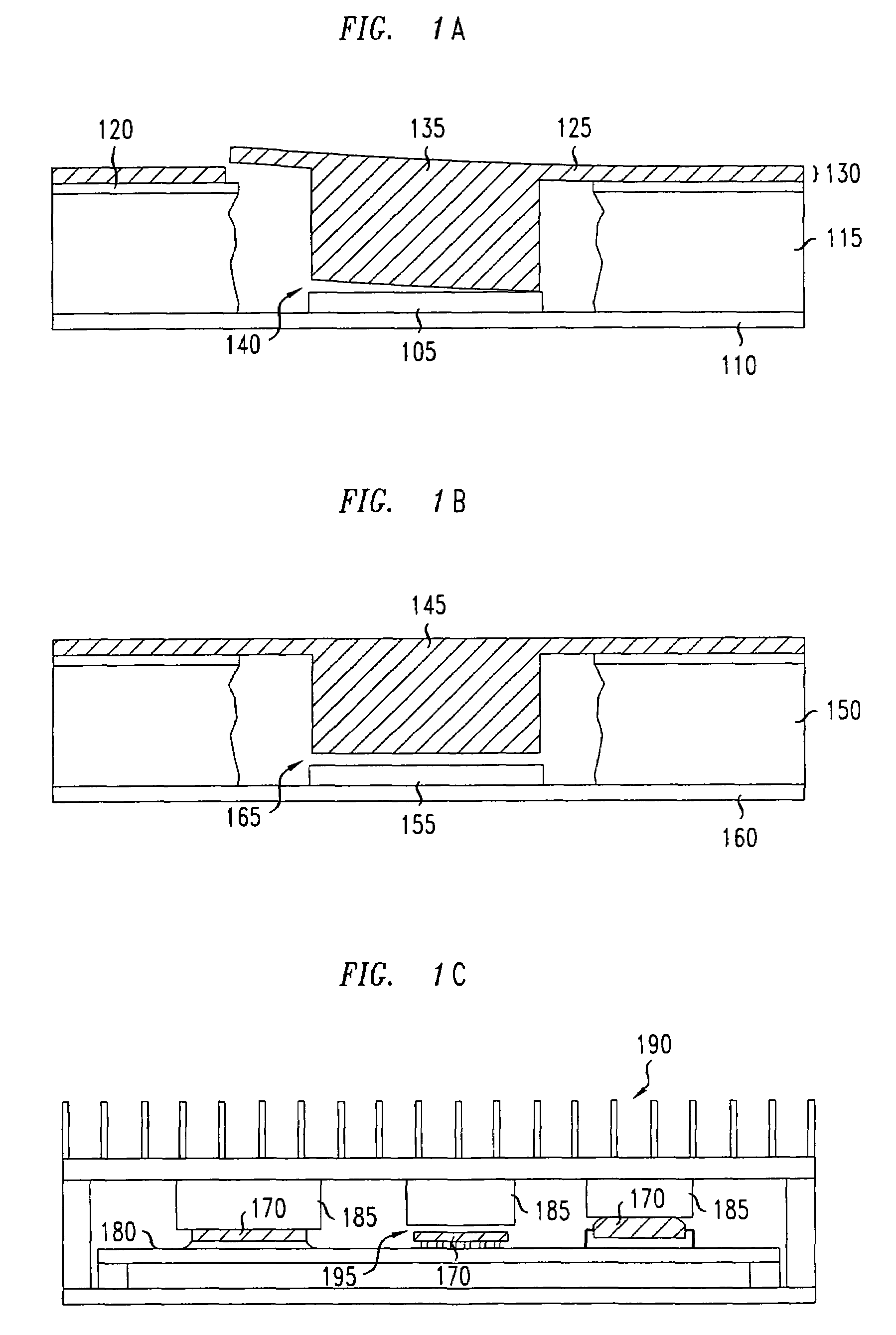
[0015]Prior to describing the various aspects and embodiments of the present invention, and to further appreciate the heat dissipation solution enabled thereby, FIGS. 1A, 1B and 1C show known heat transfer assemblies which present certain thermal management challenges, as discussed above. More particularly, the heat transfer assembly of FIG. 1A centers on the notion of dimensioning the EMI shield box such that the IC component is always “too tall”, and to use a spring-like structure to make a mechanically compliant connection between the IC component package and the lid of the EMI shield box. As will be appreciated while FIG. 1A (and FIG. 1B and FIG. 1C) is shown, illustratively, with ICs, it will be understood that there are any number of alternative heat sources which can be substituted therefore. More particularly, as shown in the cross-sectional view of FIG. 1A, IC 105 is mounted to PCB 110 which is, in turn, enclosed within EMI shield box 115 having lid 120 (fabricated, illustr...


PUM


Abstract

A thermal management for EMI shielded circuit packs having one or more high-power components, i.e. heat sources. More particularly, a heat transfer device or assembly for EMI shielded circuit packs is provided whereby multiple components (e.g., high-power components) are cooled by individual heat sinks (i.e., each component has its own individual heat sink) which protrude into an external airflow through individual openings in the lid of the EMI shield. Mechanically-compliant, electrically-conductive gaskets are used to seal the base plates of the individual heat sinks against the lid of the EMI shield enclosure. As such, in accordance with the various embodiments, the conductive gaskets establish a compliance layer which accommodates any variation in the heights of the individual components, thereby, allowing optimum thermal contact between the components and their respective heat sinks without compromising the EMI shielding.

Description

FIELD OF THE INVENTION[0001]The present invention relates generally to heat removal from electronic devices and, more specifically, to improved thermal management for electronic devices mounted in electromagnetic interference (EMI) shielded circuit packs.BACKGROUND OF INVENTION[0002]Circuit packs and modules typically have one or more printed circuit board (PCB)-mounted integrated circuits (ICs) that dissipate enough heat that cooling by simple, un-enhanced natural convection, radiation and / or by heat conduction through the PCB is insufficient to keep junction temperatures below maximum operating limits. Generally, cooling of these ICs may be obtained by thermally connecting them to heat-dissipating structures, such as heat sinks, which in turn may be cooled by forced air when necessary.[0003]Cooling using this general technique, however, is not always easy to achieve. For instance, variations in IC stack-up height and parallelism to the PCB present notable problems. For example, ci...

Claims


Application Information

Patent Timeline
Patent Type & Authority Patents(United States)
IPC IPC(8): H05K7/20
CPCH05K7/20436H05K9/0033
Inventor BOLLE, CRISTIAN AHODES, MARC SCOTTKOLODNER, PAUL ROBERT
Owner WSOU INVESTMENTS LLC
Why Eureka
Try Eureka