Floating body-type DRAM cell with increased capacitance

a dram cell and capacitance technology, applied in the field of float body-type dram cells with increased capacitance, can solve the problems of high yield, high cost, and complicated fabrication process, and achieve the effect of high yield, long data holding time, and easy formation

Inactive Publication Date: 2007-08-14
KK TOSHIBA
View PDF9 Cites 99 Cited by
  • Summary
  • Abstract
  • Description
  • Claims
  • Application Information

AI Technical Summary

Problems solved by technology

Also, since a capacitor must be formed in the 1T-1C DRAM, the fabrication process complicates, and the cost increases.
Unfortunately, even when these structures are used, it is difficult to form an FBC having a sufficiently long data holding time and high yield.

Method used


Image

  • Floating body-type DRAM cell with increased capacitance
  • Floating body-type DRAM cell with increased capacitance
  • Floating body-type DRAM cell with increased capacitance

Examples


first embodiment

(1) Semiconductor Device

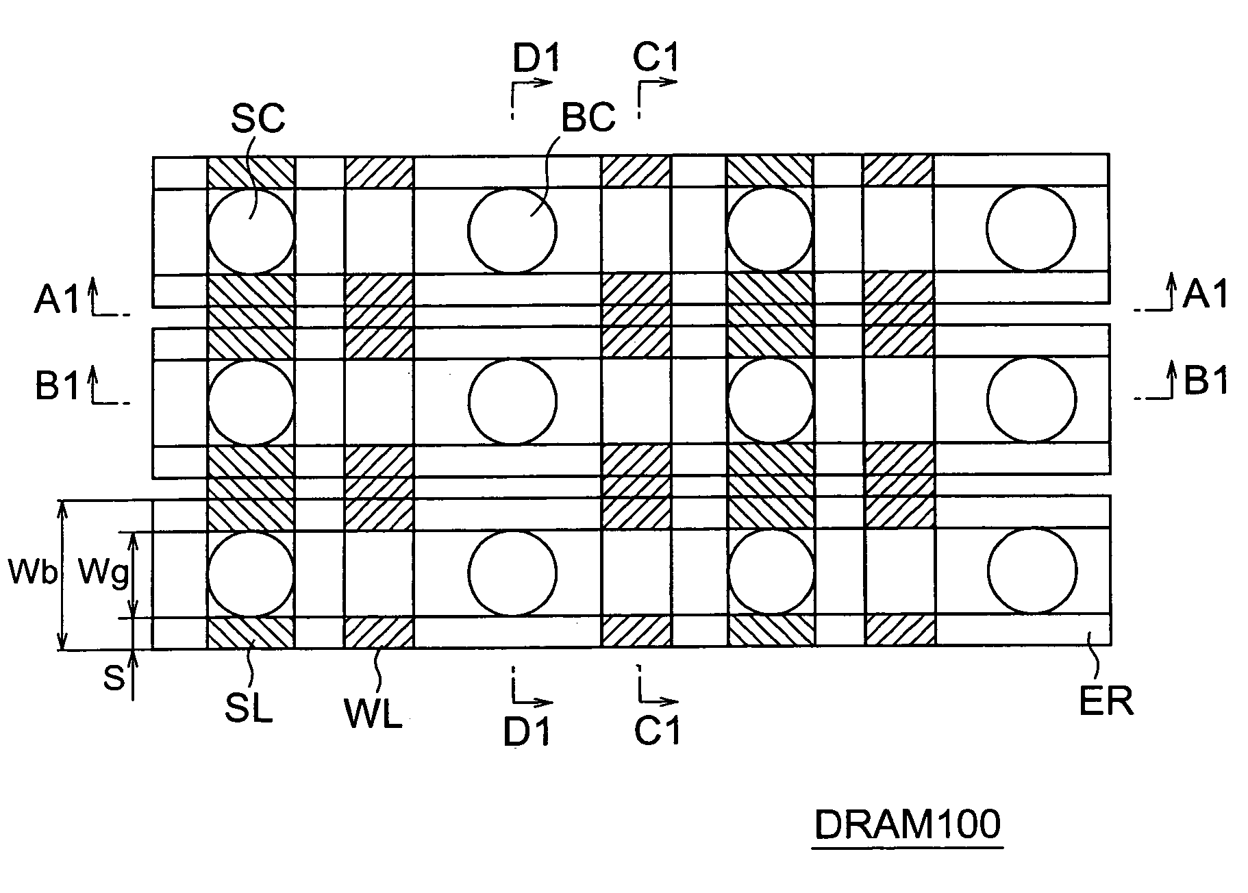
[0154]FIG. 1 shows the planar arrangement of a DRAM 100 as a semiconductor device according to the first embodiment of the present invention.

[0155]A peripheral circuit for controlling the DRAM 100 can also be formed in the periphery of the DRAM 100. The DRAM 100 includes word lines WL, source lines SL, and bit lines BL (not shown).

[0156]The word lines WL and source lines SL run substantially parallel to each other, and the bit lines BL run in a direction substantially perpendicular to the word lines WL and source lines SL.

[0157]Bit line contacts BC which electrically connect the bit lines BL (not shown) and drain regions (not shown) are formed below the bit lines BL.

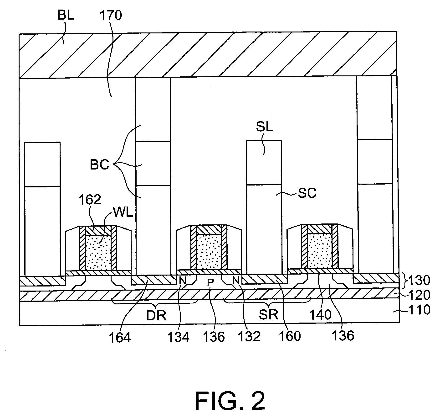
[0158]FIG. 2 shows a longitudinal sectional structure when an element region ER shown in FIG. 1 is cut along a line B1-B1. FIG. 3 shows a longitudinal sectional structure when the word line WL shown in FIG. 1 is cut along a line C1-C1.

[0159]Also, FIG. 4 shows the planar arrangement of an N-channel...

second embodiment

(3) Semiconductor Device

[0286]FIG. 26 shows the planar arrangement of a semiconductor device (DRAM 200) according to the second embodiment of the present invention.

[0287]The DRAM 200 has back gate lines BGL in addition to the constituent elements of the DRAM 100. The back gate lines BGL run substantially parallel to word lines WL.

[0288]A front gate electrode FGE (not shown) of a unit transistor is connected to the word line WL, and a back gate electrode BGE (not shown) is connected to the back gate line BGL.

[0289]FIG. 27 shows a longitudinal section taken along a line A2-A2 in FIG. 26.

[0290]Likewise, FIGS. 28, 29, and 30 illustrate longitudinal sections taken along lines C2-C2, B2-B2, and D2-D2, respectively, in FIG. 26.

[0291]As shown in FIGS. 27 to 33, particularly, in FIG. 29, in the semiconductor device according to the second embodiment, the back gate electrode BGE is formed below a body region 336 in the longitudinal section along the word lines WL.

[0292]A back gate insulating ...

third embodiment

(5) Semiconductor Device

[0323]A DRAM 300 according to the third embodiment of the present invention will be described below with reference to the accompanying drawings.

[0324]FIG. 71 shows the longitudinal sectional structure, cut along the longitudinal direction of word lines WL, of an FBC included in the DRAM 300.

[0325]In the DRAM 300, as in the first embodiment, the corners on the two sides of the upper surface of a body region are covered with shoulders having a width S and height H on the two sides of a T-shaped STI oxide film 411.

[0326]This increases the difference between drain currents when data “0” and “1” are read out, and extends the data holding time.

[0327]Also, that central upper surface portion of a body region 436, which is not covered with the shoulders of the STI oxide film 411 contains an impurity (counter impurity) 480 having a conductivity type opposite to that of the bottom portion. This lowers the threshold voltage of a transistor, and implements a low-power-con...


PUM


Abstract

A semiconductor memory device includes transistors, each including a first-conductivity-type semiconductor layer formed on a semiconductor substrate via a first insulating film, a second-conductivity-type source / drain regions formed in the semiconductor layer, a first-conductivity-type body region formed between the source region and the drain region in the semiconductor layer, the body region being electrically floating, and a gate electrode formed on a surface of a central portion of the body region via a second insulating film. In a section along a word line, which connects the gate electrodes together, a length of a boundary between the central portion of the body region and the second insulating film is smaller than a length of a boundary between the body region and the first insulating film. A second-conductivity-type counter impurity is doped in a surface portion of the central portion of the body region on which the second insulating film is formed.

Description

CROSS REFERENCE TO RELATED APPLICATION[0001]This application is based upon and claims benefit of priority under 35 USC §119 from the Japanese Patent Application No. 2004-262320, filed on Sep. 9, 2004, the entire contents of which are incorporated herein by reference.BACKGROUND OF THE INVENTION[0002]The present invention relates to a semiconductor device and a method of fabricating the same.[0003]Semiconductor memories such as DRAMs are more and more down-scaled in recent years. 1T-1C (1 Transistor-1 Capacitor) type DRAM, however, needs a certain area for the capacitor to ensure a storage capacitance of the capacitor. This limits the degree of down-scaling of the 1T-1C DRAM.[0004]Also, since a capacitor must be formed in the 1T-1C DRAM, the fabrication process complicates, and the cost increases.[0005]To solve these problems, a technique which forms a DRAM on an SOI (Silicon On Insulator) substrate is developed. For example, patent reference 1 or 2 (to be described later) discloses a...

Claims


Application Information

Patent Timeline
Patent Type & Authority Patents(United States)
IPC IPC(8): H01L27/01
CPCH01L27/108H01L27/10802H01L29/7841H01L27/10873H10B12/20H10B12/00H10B12/05
Inventor SHINO, TOMOAKI
Owner KK TOSHIBA
Why Eureka
Try Eureka