
Voltage variable substrate material

a voltage variable and substrate technology, applied in the field of circuit protection, can solve the problems of not being structurally free standing, vvm's from reaching their full potential, and the application of vvm is limited to the smallest possible substrate that can hold or support a quantity of vvm

Inactive Publication Date: 2007-08-21
LITTELFUSE INC
View PDF57 Cites 32 Cited by
  • Summary
  • Abstract
  • Description
  • Claims
  • Application Information

AI Technical Summary

Benefits of technology

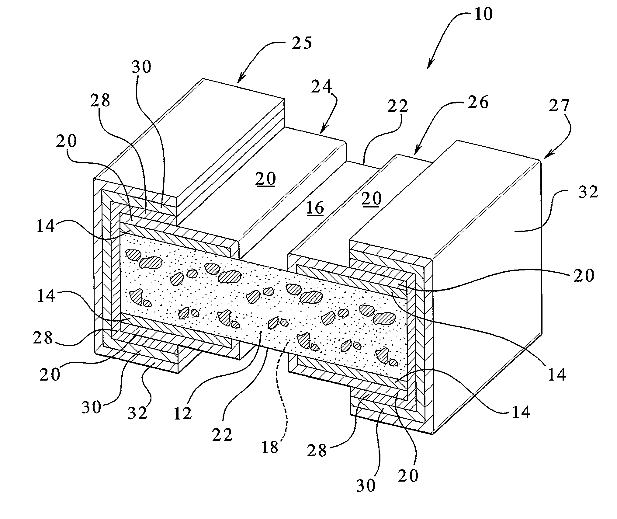
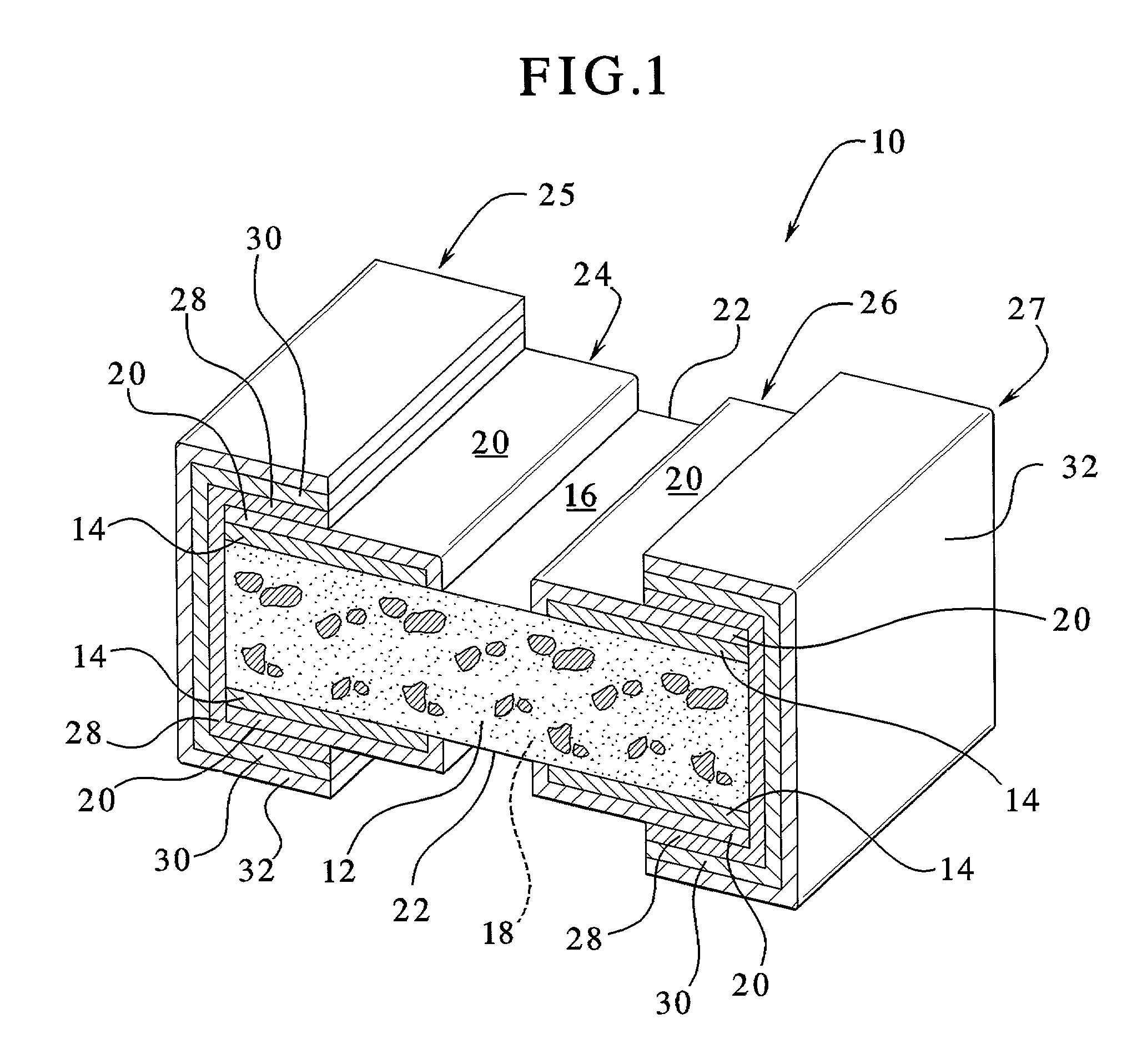
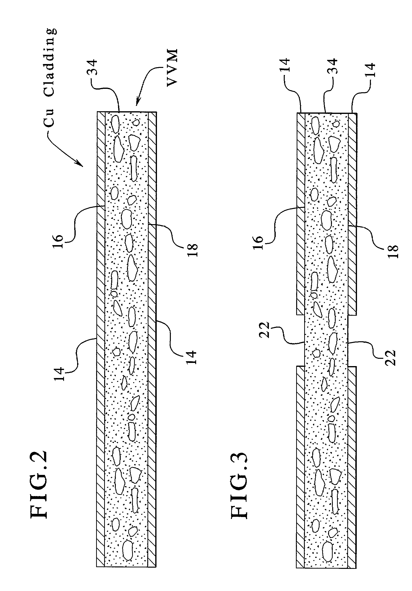
[0035]It is therefore an advantage of the present invention to provide a voltage variable material (“VVM”) that has been impregnated in a substrate.
[0036]Another advantage of the present invention is to provide a VVM substrate that operates as a printed circuit board.
[0037]A further advantage of the present invention is to provide a VVM substrate for a flexible circuit.
[0038]Yet another advantage of the present invention is to provide a VVM substrate that operates as a discrete device.
[0039]Yet a further advantage of the present invention is to provide a VVM substrate that has been extruded into a desired configuration.
[0040]Still another advantage of the present invention is to provide a VVM substrate that has been extruded along with a conductor of a data communications cable.

Problems solved by technology

One limitation keeping the known VVM's from reaching their full potential is that they are not structurally free standing.
VVM applications are thus limited to the smallest possible substrate that will hold or support a quantity of VVM, which may be too large, the wrong shape or the wrong configuration for certain applications, e.g., for certain fine pitch integrated circuits.
Other applications, such as data cabling, do not provide a convenient place to mount a substrate.

Method used


Image

  • Voltage variable substrate material
  • Voltage variable substrate material
  • Voltage variable substrate material

Examples


Embodiment Construction

[0056]The voltage variable material (“VVM”) of the present invention is self-supporting and self-standing. That is, the VVM does not need to be applied to a carrier or daughter board, and the substrate of the present invention does not need to support a separate quantity of a voltage variable material. As such, the VVM may be made in minute quantities, e.g., for application in an 0402 package size. The VVM is characterized by being either rigid or semi-rigid. Importantly, the VVM of the present invention has a structural integrity that is sufficient to mount all types of electrical components directly to the VVM, including but not limited to electrodes, circuit board traces, resistors, capacitors, integrated circuits, connectors and the like. The present invention includes portions or all of a printed circuit board having one or more layers of the VVM substrate of the present invention. That is, the VVM substrate of the present invention can have any length and width that printed ci...


PUM

PropertyMeasurementUnit
Electrical conductivityaaaaaaaaaa
Electrical conductoraaaaaaaaaa
Electric potential / voltageaaaaaaaaaa

Abstract

The present invention provides an improved voltage variable material (“VVM”). More specifically, the present invention provides an improved printed circuit board substrate, an improved device having circuit protection an improved data communications cable having circuit protection and a method for mass producing devices employing the VVM substrate of the present invention. The VVM substrate eliminates the need for an intermediate daughter or carrier board by impregnating conductive particles and possibly semiconductive and / or insulative particles associated with known volatage variable materials into the varnish or epoxy resin associated with known printed circuit board substrates.

Description

BACKGROUND OF THE INVENTION[0001]The present invention relates to circuit protection. More particularly, the present invention relates to an improved voltage variable material (“VVM”).[0002]Electrical overstress transients (“EOS transients”) produce high electric fields and high peak powers that can render circuits or the highly sensitive electrical components in the circuits, temporarily or permanently non-functional. EOS transients can include transient voltages or current conditions capable of interrupting circuit operation or destroying the circuit outright. EOS transients may arise, for example, from an electromagnetic pulse, an electrostatic discharge, lightning, a build-up of static electricity or be induced by the operation of other electronic or electrical components. An EOS transient can rise to its maximum amplitude in subnanosecond to microsecond times and have repeating amplitude peaks.[0003]The peak amplitude of the electrostatic discharge transient wave (“ESD event”) ...

Claims


Application Information

Patent Timeline
IPC IPC(8): H05K1/03H01B1/00H01C1/00H01C7/10H01C7/02H01C7/105H01C7/12H05K1/02H05K1/16
CPCH01C7/027H01C7/12H05K1/0257H05K1/0373H01C7/105Y10T29/49172H05K1/0259H05K1/167H05K2201/0209H05K2201/0215H05K2201/0323H05K2201/0329H05K2201/0738Y10S428/901Y10T29/49124
Inventor HARRIS, IV, EDWIN JAMES
Owner LITTELFUSE INC
Learn More