Vertical GaN-based LED and method of manufacturing the same

a technology of vertical gan-based led and light-emitting diodes, which is applied in the direction of semiconductor/solid-state device manufacturing, electrical apparatus, and semiconductor devices. it can solve the problems of poor thermal conductivity, limit in reducing manufacturing costs, and rigid non-conducting substrate of apphire substrate, etc., to achieve enhanced current diffusion effect, reduce contact resistance and operating voltage, and high-efficiency

Active Publication Date: 2007-08-21
SAMSUNG ELECTRONICS CO LTD
View PDF4 Cites 33 Cited by
  • Summary
  • Abstract
  • Description
  • Claims
  • Application Information

AI Technical Summary

Benefits of technology

[0016]An advantage of the present invention is that it provides a vertical GaN-based LED, in which a surface polarity of a GaN-based semiconductor layer contacting an n-electrode is controlled to reduce the contact resistance and the operating voltage, and a current diffusion effect is enhanced to obtain the high-output characteristics.
[0017]The present invention also provides a method of manufacturing the vertical GaN-based LED.
[0018]Additional aspect and advantages of the present general inventive concept will be set forth in the description which follows and, in part, will be obvious from the description, or may be learned by practice of the general inventive concept.
[0019]According to an aspect of the invention, a vertical GaN-based LED includes: an n-electrode; an AlGaN layer formed under the n-electrode; an undoped GaN layer formed under the AlGaN layer to provide a two-dimensional electron gas (2DEG) layer to a junction interface of the AlGaN layer; a GaN-based LED structure including an n-type GaN layer, an active layer, and a p-type GaN layer that are sequentially formed under the undoped GaN layer; a p-electrode formed under the GaN-based LED structure; and a conductive substrate formed under the p-electrode.
[0020]According to another aspect of the invention, the surface of the AlGaN layer contacting the n-electrode has a Ga-face structure in which nitrogen nitride (N) elements are disposed on a vertical uppermost layer of gallium (Ga) elements. Accordingly, the contact resistance of the n-electrode can be reduced. Also, a piezoelectric effect is directed toward the AlGaN layer, i.e., the opposite direction of the n-electrode, thereby greatly enhancing the current diffusion effect of the 2DEG layer formed under the AlGaN layer.
[0021]According to a further aspect of the invention, the vertical GaN-based LED further includes a conductive junction layer formed on the p-electrode or at an interface between the p-electrode and the conductive substrate.

Problems solved by technology

Generally, a GaN-based LED is grown on a sapphire substrate, but the sapphire substrate is a rigid nonconductor and has poor thermal conductivity.
Therefore, there is a limit in reducing the manufacturing costs by reducing the size of a GaN-based LED, or improving chip characteristics such as optical power and electrostatic discharge (EDD).
Consequently, the light-generation efficiency of the LED is degraded and the lifespan of the LED is reduced.

Method used


Image

  • Vertical GaN-based LED and method of manufacturing the same
  • Vertical GaN-based LED and method of manufacturing the same
  • Vertical GaN-based LED and method of manufacturing the same

Examples


Embodiment Construction

[0038]Reference will now be made in detail to the embodiments of the present general inventive concept, examples of which are illustrated in the accompanying drawings, wherein like reference numerals refer to like elements throughout. In the drawings, the thicknesses of layers and regions are exaggerated for clarity. The embodiments are described below in order to explain the present general inventive concept by referring to the figures.

[0039]Hereinafter, preferred embodiments of the present invention will be described in detail with reference to the accompanying drawings.

[0040]Structure of Vertical GaN-based LED

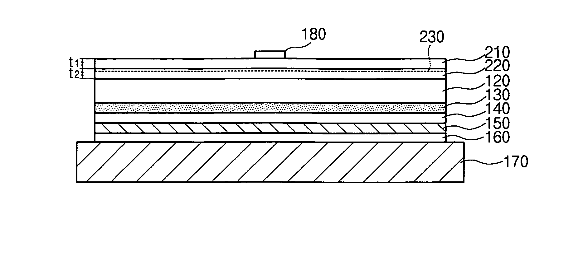
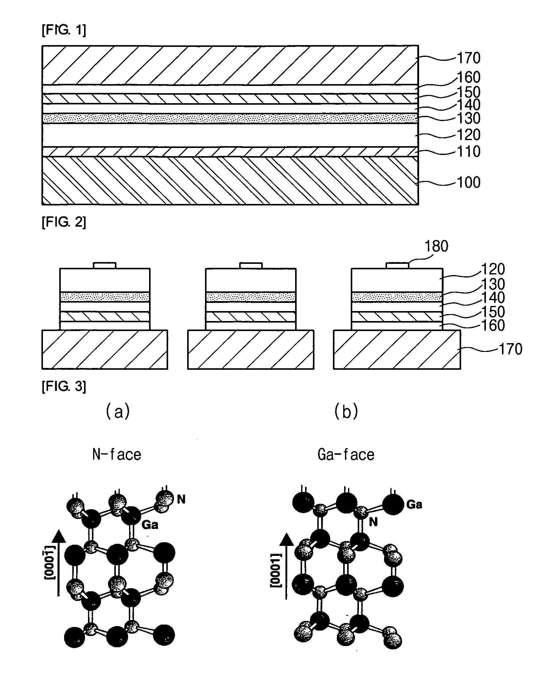
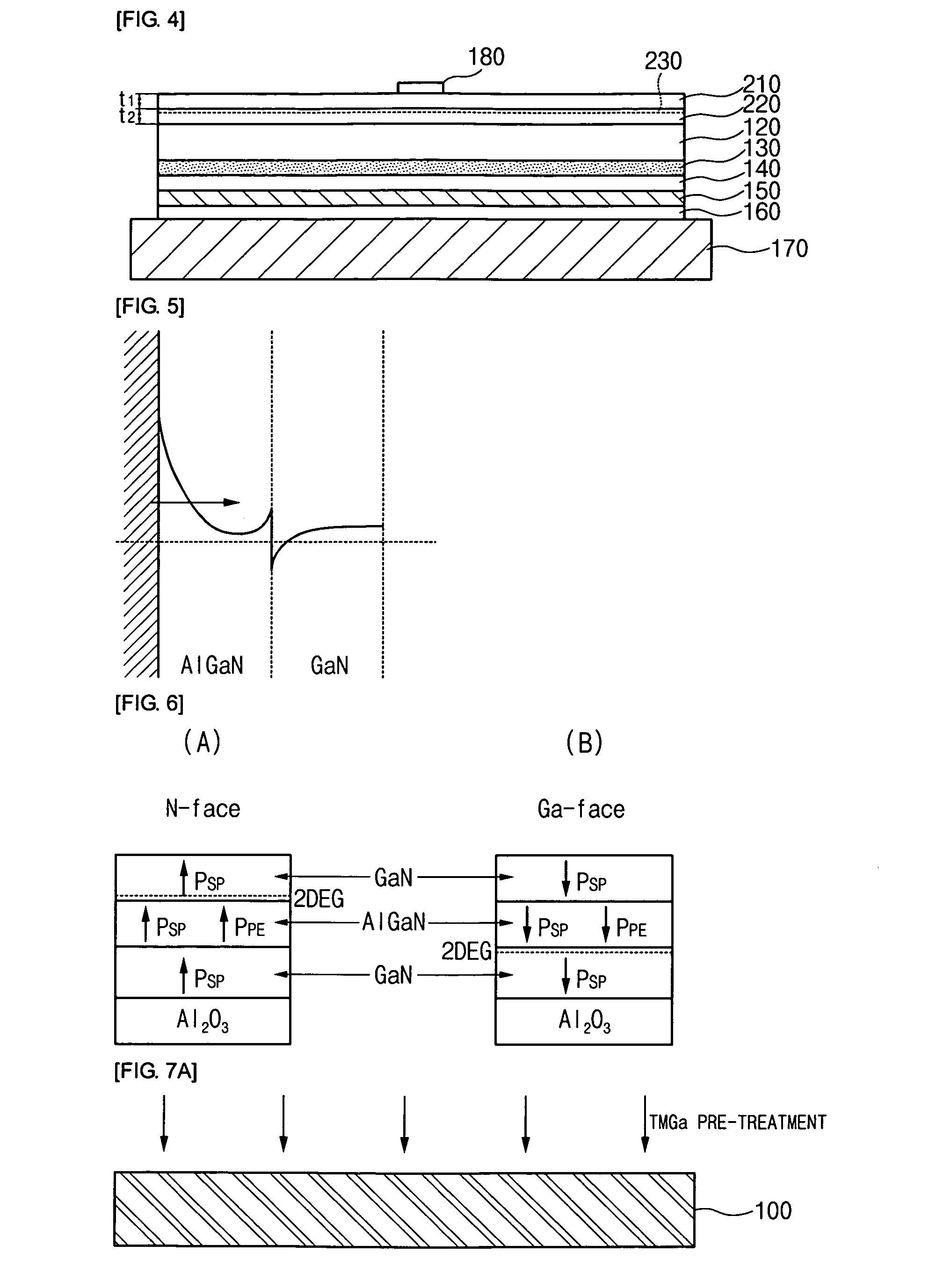
[0041]The structure of a vertical GaN-based LED according to an embodiment of the present invention will be described in detail with reference to FIGS. 4 to 6.

[0042]FIG. 4 is a sectional view of a vertical GaN-based LED according to an embodiment of the present invention. FIG. 5 is an energy band diagram illustrating an AlGaN / GaN hetrojunction band structure used in the vert...


PUM


Abstract

Provided are a vertical GaN-based LED and a method of manufacturing the same. The vertical GaN-based LED includes an n-electrode. An AlGaN layer is formed under the n-electrode. An undoped GaN layer is formed under the AlGaN layer to provide a two-dimensional electron gas layer to a junction interface of the AlGaN layer. A GaN-based LED structure includes an n-type GaN layer, an active layer, and a p-type GaN layer that are sequentially formed under the undoped GaN layer. A p-electrode is formed under the GaN-based LED structure. A conductive substrate is formed under the p-electrode.

Description

CROSS-REFERENCE TO RELATED APPLICATIONS[0001]This application claims the benefit of Korean Patent Application No. 2005-0066616 filed with the Korea Industrial Property Office on Jul. 22, 2005, the disclosure of which is incorporated herein by reference.BACKGROUND OF THE INVENTION[0002]1. Field of the Invention[0003]The present invention relates to a vertical (i.e., vertical-electrode type) GaN-based light emitting diode (LED) and a method of manufacturing the same. In the vertical GaN-based LED, when a negative electrode (n-electrode) contacts an n-type GaN layer from which a sapphire substrate has been removed by a laser lift-off (LLO) process, a contact resistance and an operating voltage are reduced to enhance a current diffusion effect.[0004]2. Description of the Related Art[0005]Generally, a GaN-based LED is grown on a sapphire substrate, but the sapphire substrate is a rigid nonconductor and has poor thermal conductivity. Therefore, there is a limit in reducing the manufacturi...

Claims


Application Information

Patent Timeline
Patent Type & Authority Patents(United States)
IPC IPC(8): H01L29/22H01L29/24H01L33/12H01L33/16H01L33/32H01L33/38
CPCH01L33/14H01L33/32H01L33/0079H01L33/16H01L33/0093
Inventor LEE, JAE HOONCHOI, HEE SEOKOH, JEONG TAKLEE, SU YEOL
Owner SAMSUNG ELECTRONICS CO LTD
Why Eureka
Try Eureka