Digital black clamp circuit in electronic imaging systems

Active Publication Date: 2007-08-21
OMNIVISION TECH INC
View PDF11 Cites 8 Cited by
  • Summary
  • Abstract
  • Description
  • Claims
  • Application Information

AI Technical Summary

Benefits of technology

[0029]9. This invention uses two, or more digital comparators to provide a hysteresis to prevent the loop from hunting. This has the advantage o

Problems solved by technology

As the imager is operated, it heats up, due to its' internal power dissipation.
This solution also consumes the power to run the microprocessor and the microprocessor machine cycles which are not available for other functions.
The first stage black clamp does not correct for residual errors that can be caused by the PGA and also does not correct for errors that are caused by the analog-to-digital (A/D) converter circuit appearing at a later stage

Method used


Image

  • Digital black clamp circuit in electronic imaging systems
  • Digital black clamp circuit in electronic imaging systems
  • Digital black clamp circuit in electronic imaging systems

Examples


Example

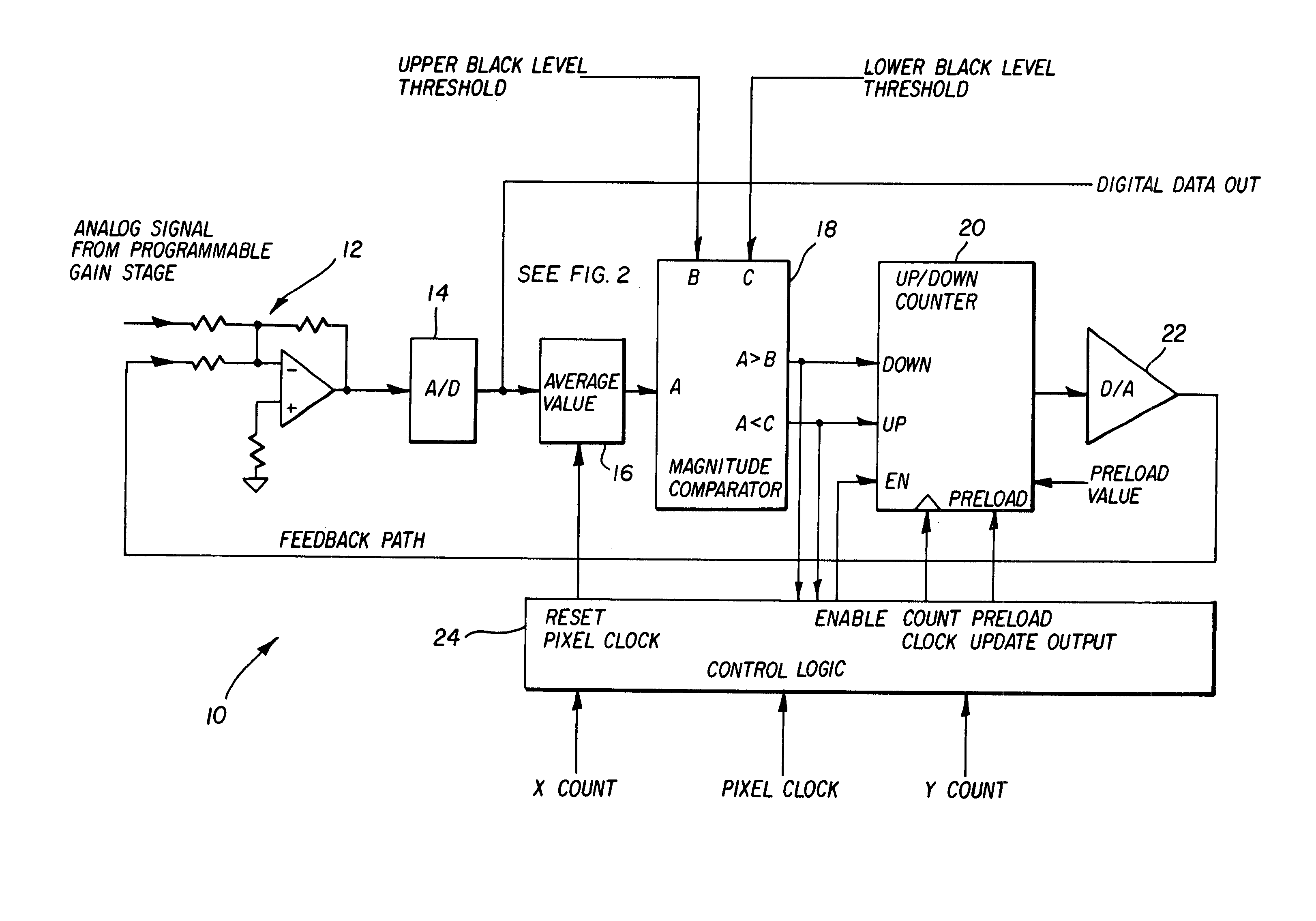
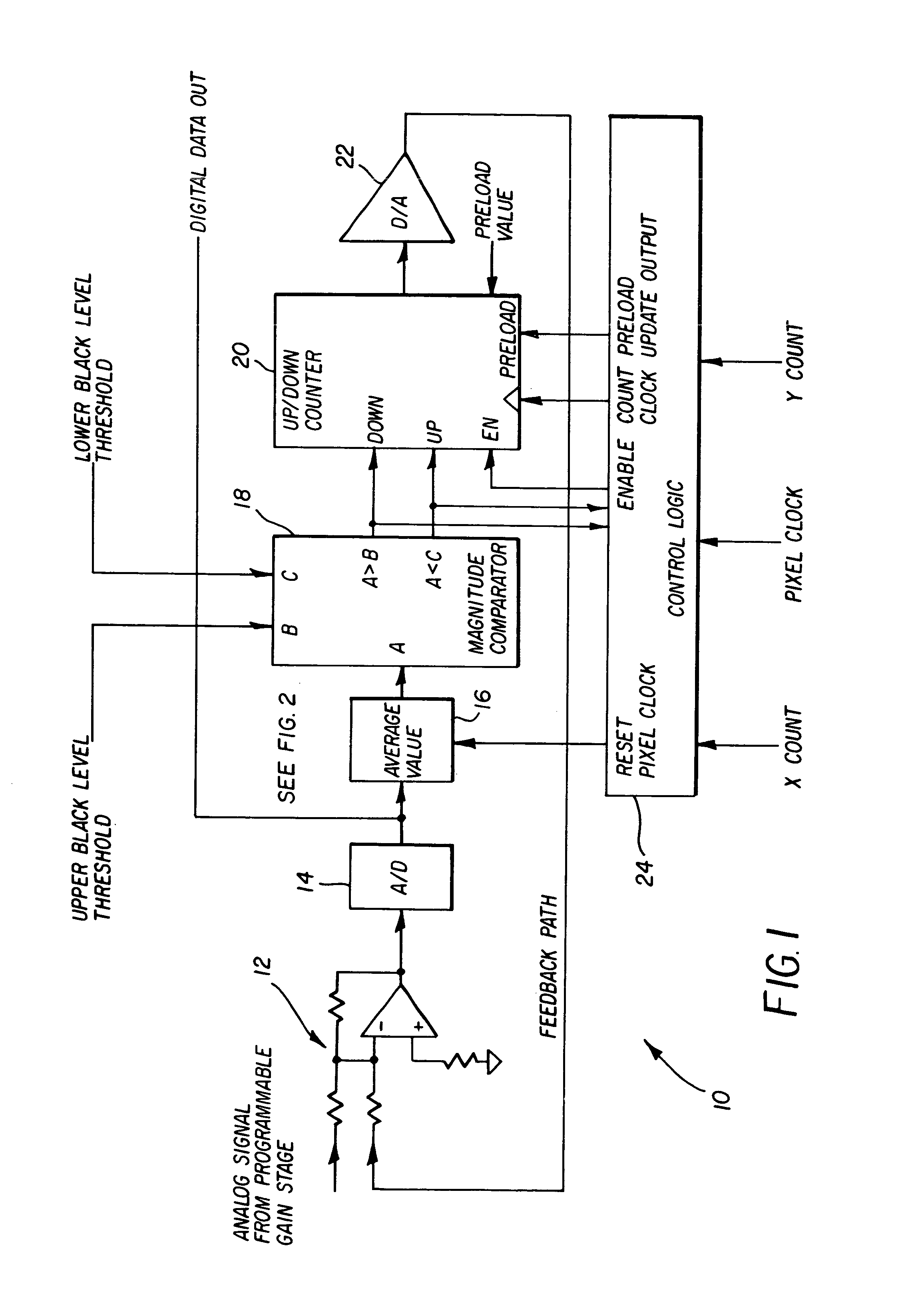
[0036]In the following description, the present invention will be described in the preferred embodiment as a hardware circuit.

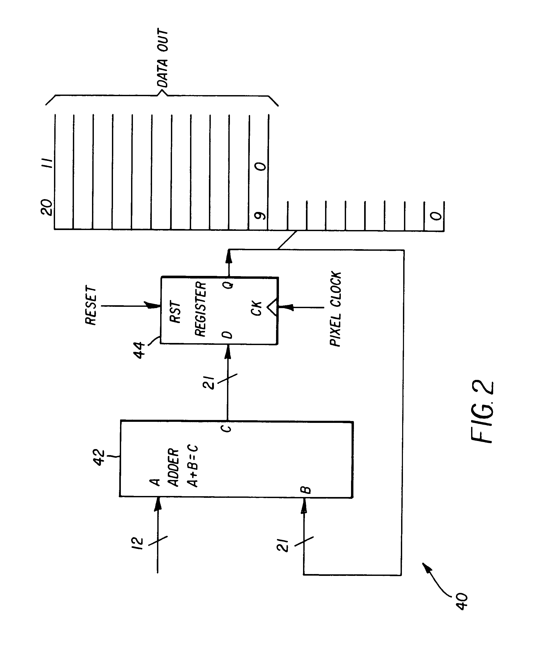
[0037]The present invention utilizes a digital average value circuit to calculate the average value of a group of black pixels. The average value is then used in a real time feedback loop that removes offset errors in the signal processing chain and establishes the correct black level in the output image data. The feedback can be either digital or analog.

[0038]The present invention removes the residual errors previously mentioned. An additional benefit of the present invention is to relieve performance requirements on the first stage black clamp. Instead of clamping too exactly at the “0” of the Programmable Gain Amplifier (PGA), the first stage clamp just needs to get “close enough to 0.” The present invention is used to remove all the offset errors up to and including that of the analog-to-digital converter.

[0039]This invention is intended for, but not rest...


PUM


Abstract

The present invention is a black clamp circuit for an electronic imager having black reference pixels. The circuit includes an average value circuit determining an average of a number of the black reference pixels, a correction circuit determining the black level correction from the average, and a modifier circuit modifying image pixels with the black level. The average value is used in a real time feedback loop that removes offset errors in the signal processing chain and establishes a corrected black level in output image data. The feedback can be either digital or analog. The correction circuit can include a comparator that allows a hysteresis in the feedback to avoid hunting as well as multiple levels of feedback based on several thresholds. The corrected black level can also be controlled by a digital transfer function. The black clamp circuit can be used for a series of images, an image frame and an image line.

Description

FIELD OF THE INVENTION[0001]The invention relates generally to the field of imaging, and in particular to black level clamping in digital sensor imaging. More specifically, the invention relates to a black clamp circuit that tracks the changes in black level (due to noise and dark current) and removes errors in the signal processing and does so in real time.BACKGROUND OF THE INVENTION[0002]Typically, a border of an image-sensing array, such as a Charge Coupled Device (CCD) imager or a CMOS imager, is surrounded with a number of rows and columns of light shielded, or black, pixels. These pixels provide black reference information or black pixel data to stabilize downstream image processing and establish the correct value for black in the output image. Charged Coupled Device Imager (CCD) and CMOS Imager signal processing chains have a need to establish and maintain the black reference in the signal processing chain.[0003]The image-sensing array black pixel data contains a dark current...

Claims


Application Information

Patent Timeline
IPC IPC(8): H04N9/64H04N5/18H04N5/361
CPCH04N5/185H04N5/361H04N25/63
Inventor MCDERMOTT, BRUCE C.
Owner OMNIVISION TECH INC
Why Eureka
Try Eureka