Method and system for performing built-in self-test routines using an accumulator to store fault information

a self-testing and accumulator technology, applied in the field of integrated circuit die testing and repair, can solve the problems of high production cost, high production cost, and high cost of test development, and achieve the effect of improving yield

Inactive Publication Date: 2007-08-21
AVAGO TECH INT SALES PTE LTD
View PDF3 Cites 70 Cited by
  • Summary
  • Abstract
  • Description
  • Claims
  • Application Information

AI Technical Summary

Benefits of technology

[0054]One advantage of the present invention is that a single BIST process can be run under all of the proposed stress conditions.
[0055]Another advantage of the present invention is that repair information (i.e., faulty/defective memory address locations) is accumulated under different stress conditions.
[0056]A further advantage of the invention is that the accumulation of all repair solutions ensures that all failure information

Problems solved by technology

Because of the increasing complexity of new designs, test development costs now account for a large percentage of the total ASIC development cost.
This testing is necessary because perfect yields are difficult to achieve.
It is not uncommon for a certain percentage of unpackaged ASIC die to contain memory cells which fail testing processes, due largely to non-systemic manufacturing defects and degradation faults.
Such manufacturing issues are likely to increase as process geometries continue to shrink and the density of memory cells increases.
While this methodology does not utilize any chip area other than some simple multiplexing circuitry, it is limited to on-chip memories and other circuitry accessible via I/O pins.
Another drawback of this approach is that ATE capabilities are generally not available to end users once the devices have been shipped, making it difficult to detect faults occurring after shipment.
However, these techniques may leave integrated circuits useless if the repaired memories become defective after shipment from the manufacturing site.
This approach may not work for integrated circuits incorporating embedded memories and BIST/BISR capabilities, as test and repair routines are generally executed only at power-up.
Running current BIST algorithms may not adequately detect memory locations having faults that are dependent

Method used


Image

  • Method and system for performing built-in self-test routines using an accumulator to store fault information
  • Method and system for performing built-in self-test routines using an accumulator to store fault information
  • Method and system for performing built-in self-test routines using an accumulator to store fault information

Examples


Embodiment Construction

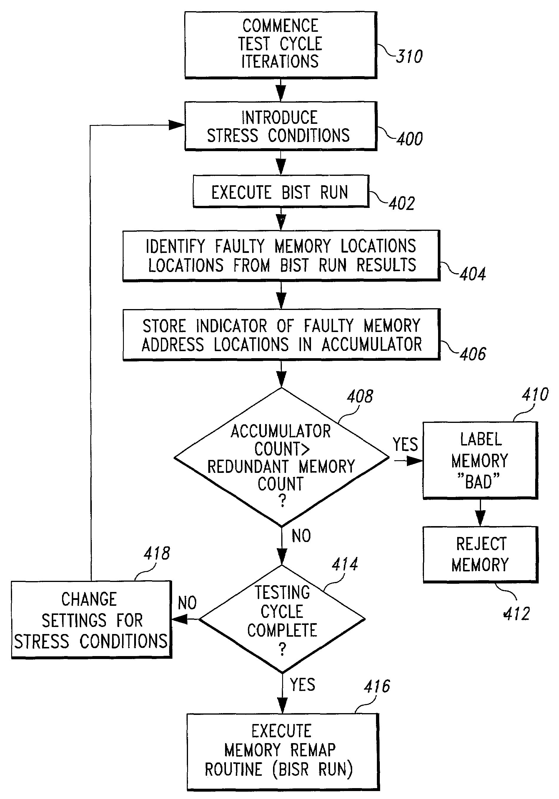
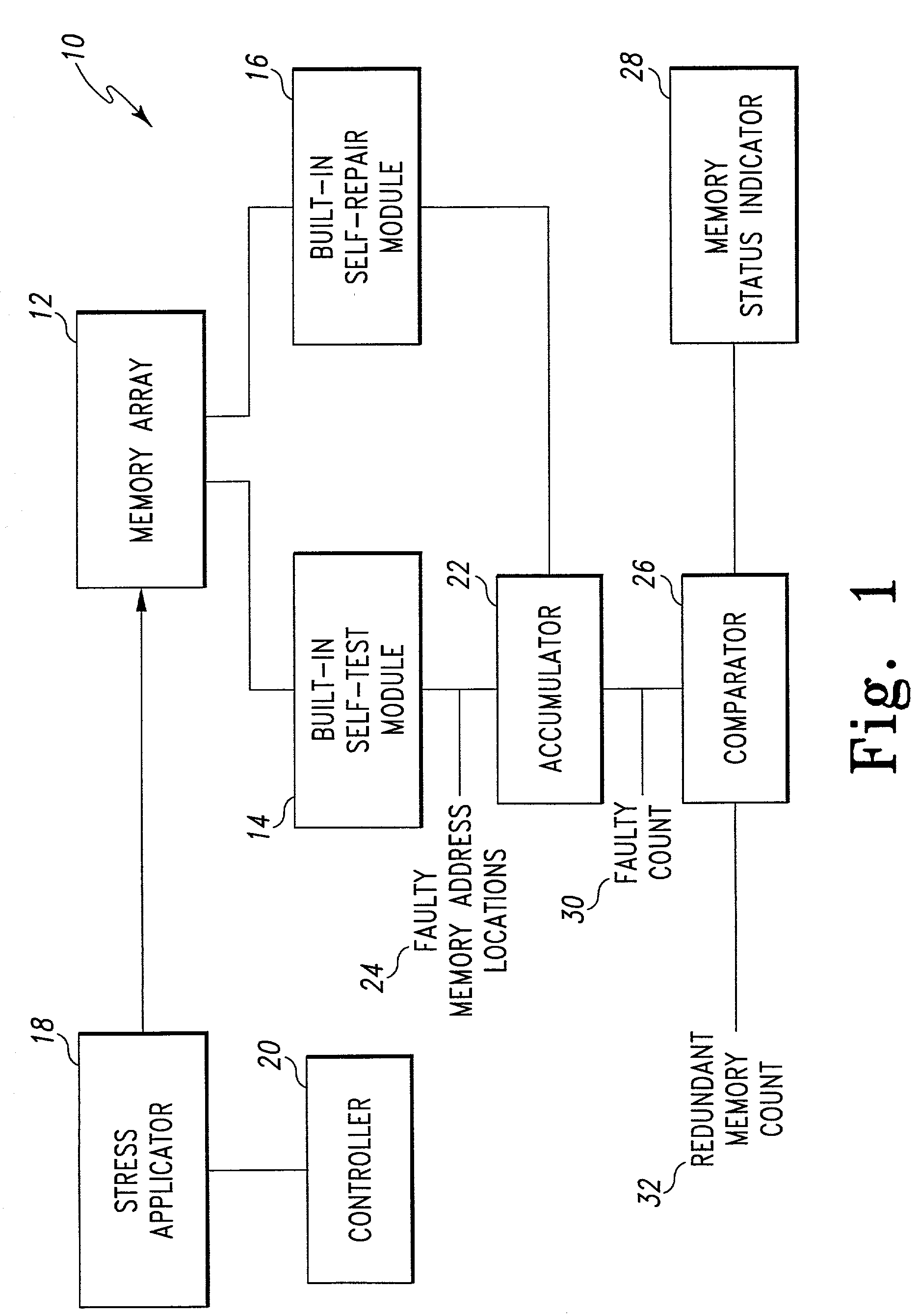
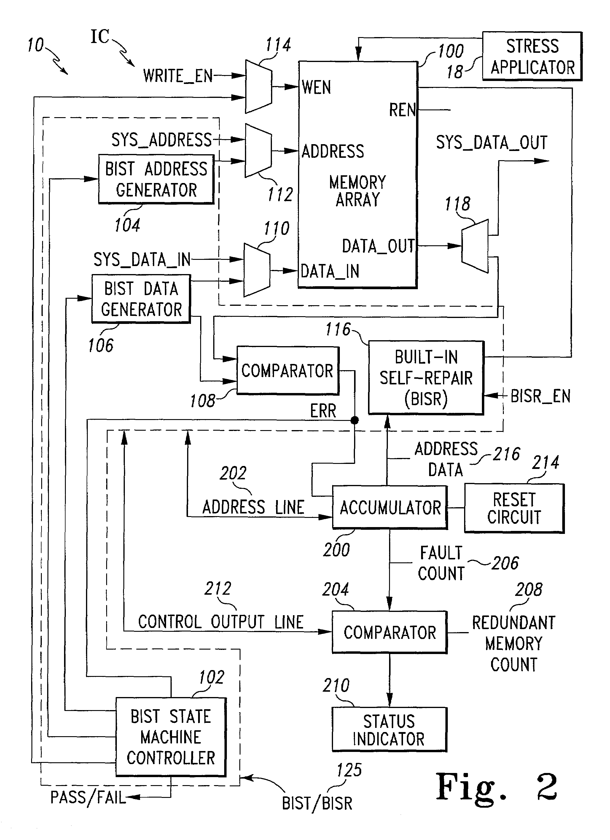
[0064]Referring now to the drawings and particularly to FIG. 1, there is shown a simplified block diagram representation of an integrated circuit (IC) assembly 10 for use in analyzing a memory array 12, according to one embodiment of the present invention. Preferably, IC assembly 10 is used in conjunction with a manufacturing test procedure conducted prior to delivery of the end user machine that incorporates memory array 12. More particularly, the test procedure is preferably performed at the wafer stage prior to singulation. IC assembly 10 finds particular use when memory array 12 is an embedded storage device.

[0065]Although IC assembly 10 is described in conjunction with memory array 12, this should not be seen in limitation of the present invention as it should be apparent that the present invention may be practiced with other devices that include, but are not limited to, computer-related modules, logic circuitry, electrical components, and other apparatus having any combination...


PUM


Abstract

A test system includes a built-in self-test (BIST) circuit and a stress applicator for use in analyzing a memory array. The stress applicator applies a selective set of stress factors to the memory array, such as temperature and voltage conditions. The BIST circuit executes a test routine on the memory array to detect the presence of any faulty memory address locations that may arise under the prevailing stress condition. A full testing cycle involves iterative repetition of the functions performed by the stress applicator and BIST circuit, with variations in the stress factors across the testing iterations. An accumulator cumulatively stores the fault information generated by the BIST circuit during each testing iteration. Following completion of the testing cycle, a repair operation is performed by a built-in self-repair (BISR) circuit to remap the faulty memory address locations indicated by the accumulator to redundant memory address locations.

Description

BACKGROUND OF THE INVENTION[0001]1. Field of the Invention[0002]The present invention relates to the testing and repair of integrated circuit dies, and, more particularly, to a method and system for cumulatively storing memory fault information produced during successive iterations of a manufacturing test cycle involving a stress procedure that introduces stress factors into the die and a test routine that executes built-in self-test (BIST) algorithms, followed by an overall global self-repair procedure that is conducted using the cumulatively stored fault information.[0003]2. Description of the Related Art[0004]Integrated circuits have become key components of many consumer and commercial electronic products, often replacing discrete components and enhancing functionality. The semiconductor processing technologies that produce these integrated circuits have advanced to the point where complete systems, including memories, can be reduced to a single integrated circuit or application...

Claims


Application Information

Patent Timeline
IPC IPC(8): G01R31/28
CPCG11C29/56G11C29/56008
Inventor AGRAWAL, GHASI R.PURI, MUKESH K.SCHWARZ, WILLIAM
Owner AVAGO TECH INT SALES PTE LTD
Why Eureka
Try Eureka