Semiconductor wafer regenerating system and method

a technology of semiconductor wafers and regenerating systems, applied in the direction of abrasive blasting machines, manufacturing tools, abrasive equipment, etc., can solve the problems of reducing the efficiency of regenerating systems, and reducing so as to reduce the planarity and purity of the wafer, reduce the cost of regenerating systems, and reduce the effect of regenerating

Inactive Publication Date: 2007-08-28
SILFINE
View PDF12 Cites 21 Cited by
  • Summary
  • Abstract
  • Description
  • Claims
  • Application Information

AI Technical Summary

Benefits of technology

[0017]According to the present invention, it is possible to remove the circuit patterns formed in the semiconductor wafer in a simple, rapid, and efficient manner, thus regenerating the semiconductor wafer. The semiconductor wafer regenerated by the present invention can be used in applications which requires less planarity and purity of the wafer than the integrated circuits: e.g., the fabrication of solar cells or the like. Since the patterns of the silicon wafer is removed in a dry method of using a grit blasting technique, the present invention makes it possible to easily treat pulverulent bodies (P) such as chips and dusts produced in the pattern removal process. This allows the grits and chips to be reused, which makes the pattern removal process cost-effective. In addition, the silicon wafer can be supplied to the grit blaster in an automated fashion, which helps to increase the yield rate to a great extent.

Problems solved by technology

The discarded wafers which failed to pass the wafer test or device test retains circuit patterns and cannot be used for another purpose, and thus are typically crushed into pieces and scrapped under the ground.
Such disposal of discarded wafers results in waste of expensive resources, wafer, and may bring about environment contamination.
However, the disclosed method may be inefficient in that not so few process steps are involved in the regenerating process, which makes this method time-consuming.
Further, simply polishing and immersing the wafer in mixed acids cannot guarantee the complete removal of ion-implanted region showing physical characteristics different from that of pure silicon and trenches deeply formed into the surface.
Besides, the use of several kinds of acids increases the cost for regenerating the wafer.
As a result, this method may be much more time-consuming and inefficient.
As mentioned above, the conventional methods show low productivity in regenerating semiconductor wafers and are costly due to the use of a large quantity of chemicals and abrasives.
Thus, the prior art wafer regenerating techniques provide little benefit from the economic point of view.

Method used


Image

  • Semiconductor wafer regenerating system and method
  • Semiconductor wafer regenerating system and method
  • Semiconductor wafer regenerating system and method

Examples


Embodiment Construction

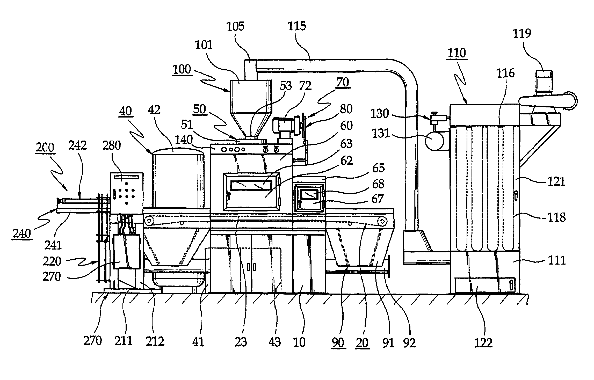
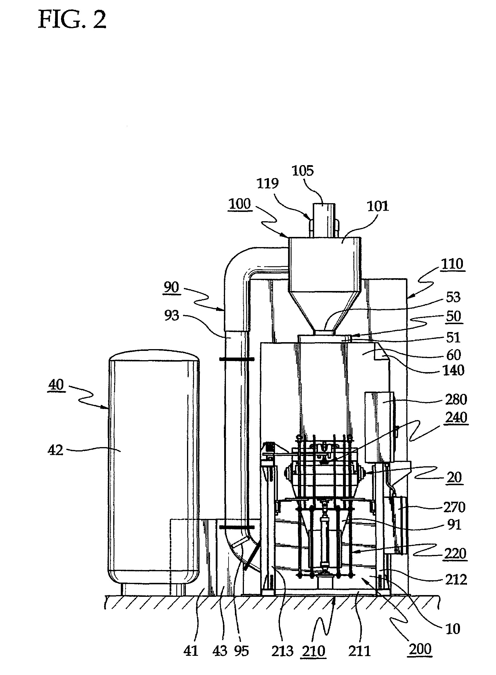
[0035]Referring to FIGS. 1 and 2, a semiconductor wafer regenerating system (referred to as “wafer regenerating system” hereinbelow) according to a preferred embodiment of the present invention includes a frame 10 above which is provided a mesh conveyor 20 for transferring silicon wafer 1. Also, above the frame 10 are provided a blasting booth 60 and a cleaning booth 65 enclosing upper side and the lateral side of mesh conveyor 20 in a line. Inside the blasting booth 60 is provided a grit blaster which blasts grits along with compressed air onto the silicon wafer to remove patterns formed on the silicon wafer. Meanwhile, inside the cleaning booth 65 is provided a cleaning nozzle which blows off impurities remaining on the wafer surface using compressed air.

[0036]On the other hand, underneath the mesh conveyor 20 is provided a collecting unit 90 which collects grits bypassing the wafer, grits bounced by the wafer after colliding against the wafer to remove the patterns, scraps of gri...


PUM

PropertyMeasurementUnit
thickaaaaaaaaaa
grain sizeaaaaaaaaaa
diameteraaaaaaaaaa

Abstract

A semiconductor wafer regenerating system is capable of easily and efficiently removing fabricating patterns formed on a semiconductor wafer to enable reuse of the semiconductor wafer. The system, which removes patterns of the semiconductor wafer in a dry manner by using blasting grit, includes a mesh conveyor, a grit blaster, a swinging element, a collecting element, a separating element, and a dust collector. The mesh conveyor transports the semiconductor wafer so that the patterns face upward. The grit blaster is installed above the mesh conveyor and has at least one blasting nozzle for blasting grits toward the semiconductor wafer to remove the patterns from the semiconductor wafer. The swinging element swings the blasting nozzle in a plane perpendicular to a transporting path of the semiconductor wafer along the mesh conveyor. The collecting element underneath the mesh conveyor collects pulverulent bodies including grits, chips, and dusts falling from the mesh conveyor. The separating element is connected to the collecting element to separate the grits and chips from the dusts. The dust collector is connected to the separating element to collect the dusts separated by the separating element.

Description

BACKGROUND OF THE INVENTION[0001]1. Field of the Invention[0002]The present invention relates to a semiconductor wafer regenerating system and method and, more specifically, to a system and method for removing patterns formed on a semiconductor wafer to enable the reuse of the semiconductor wafer.[0003]2. Description of Related Arts[0004]Semiconductor integrated circuit (IC) chips being present in everyday electrical and electronic devices are created through a multiple-step sequence of photographic and chemical processing steps, during which electronic circuits are gradually created on a wafer made of pure semiconductor material. Reviewing the semiconductor device fabrication in more detail, extremely pure semiconductor material (e.g., silicon) is grown into mono-crystalline cylindrical ingots, and the ingots are then sliced into wafers about 0.75 mm thick and polished to obtain a very flat surface. Once the wafers are prepared, transistors are formed on the silicon water using var...

Claims


Application Information

Patent Timeline
Patent Type & Authority Patents(United States)
IPC IPC(8): B24C3/04
CPCB24C3/322B24C7/0046
Inventor KIM, SUNG-SHINHAN, SANG-BONG
Owner SILFINE
Why Eureka
Try Eureka