Strained semiconductor-on-insulator structures and methods for making strained semiconductor-on-insulator structures

a technology of semiconductors and structures, applied in the field of semiconductor structures, can solve the problems of difficult replacement of silicon wafers with glass or glass-ceramic of the type, quartz itself is a relatively expensive material, and the cost of such structures has been the cost of silicon wafers, etc., to achieve enhanced performance, low cost substrates, and high efficiency

Inactive Publication Date: 2007-08-28
CORNING INC
View PDF22 Cites 15 Cited by
  • Summary
  • Abstract
  • Description
  • Claims
  • Application Information

AI Technical Summary

Benefits of technology

[0032]The semiconductor-on-insulator structures and methods for making semiconductor-on-insulator structures of the present invention result in a number of advantages over prior art. The present invention satisfies the long-standing need in the art for lower cost substrates for strained SOI structures. In addition, the invention provides novel forms for such structures. Among the numerous applications for the invention are those in such fields as optoelectronics, RF electronics, and mixed signal (analog / digital) electronics, as well as display applications, e.g., LCDs and OLEDs, where significantly enhanced performance can be achieved compared to amorphous silicon, polysilicon and unstrained silicon based devices. In addition, photovoltaics and solar cells with high efficiency are also enabled. Both the invention's novel processing techniques and its novel strained SOI structures significantly lower the cost of a strained SOI structure and thus satisfy the continuing demand in the semiconductor field for lower cost strained semiconductor devices.

Problems solved by technology

To date, a major part of the cost of such structures has been the cost of the silicon wafer which supports the oxide layer, topped by the Si thin film, i.e., a major part of the cost has been the support substrate.
Although the use of quartz as a support substrate has been mentioned in various patents (see U.S. Pat. Nos. 6,140,209; 6,211,041; 6,309,950; 6,323,108; 6,335,231; and 6,391,740), quartz is itself a relatively expensive material.
In particular, it is difficult to replace a silicon wafer with a glass or glass-ceramic of the type which can be manufactured in large quantities at low cost, i.e., it is difficult to make cost effective SOG structures.
However, the cost of strained silicon substrates can be high, because prior to the present invention, the art has not had practical techniques for making semiconductor-on-insulator structures having a strained semiconductor layer and glass or glass-ceramics as the support substrate.

Method used


Image

  • Strained semiconductor-on-insulator structures and methods for making strained semiconductor-on-insulator structures
  • Strained semiconductor-on-insulator structures and methods for making strained semiconductor-on-insulator structures
  • Strained semiconductor-on-insulator structures and methods for making strained semiconductor-on-insulator structures

Examples


example

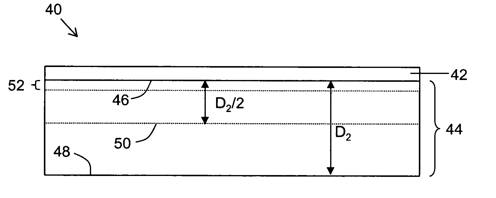
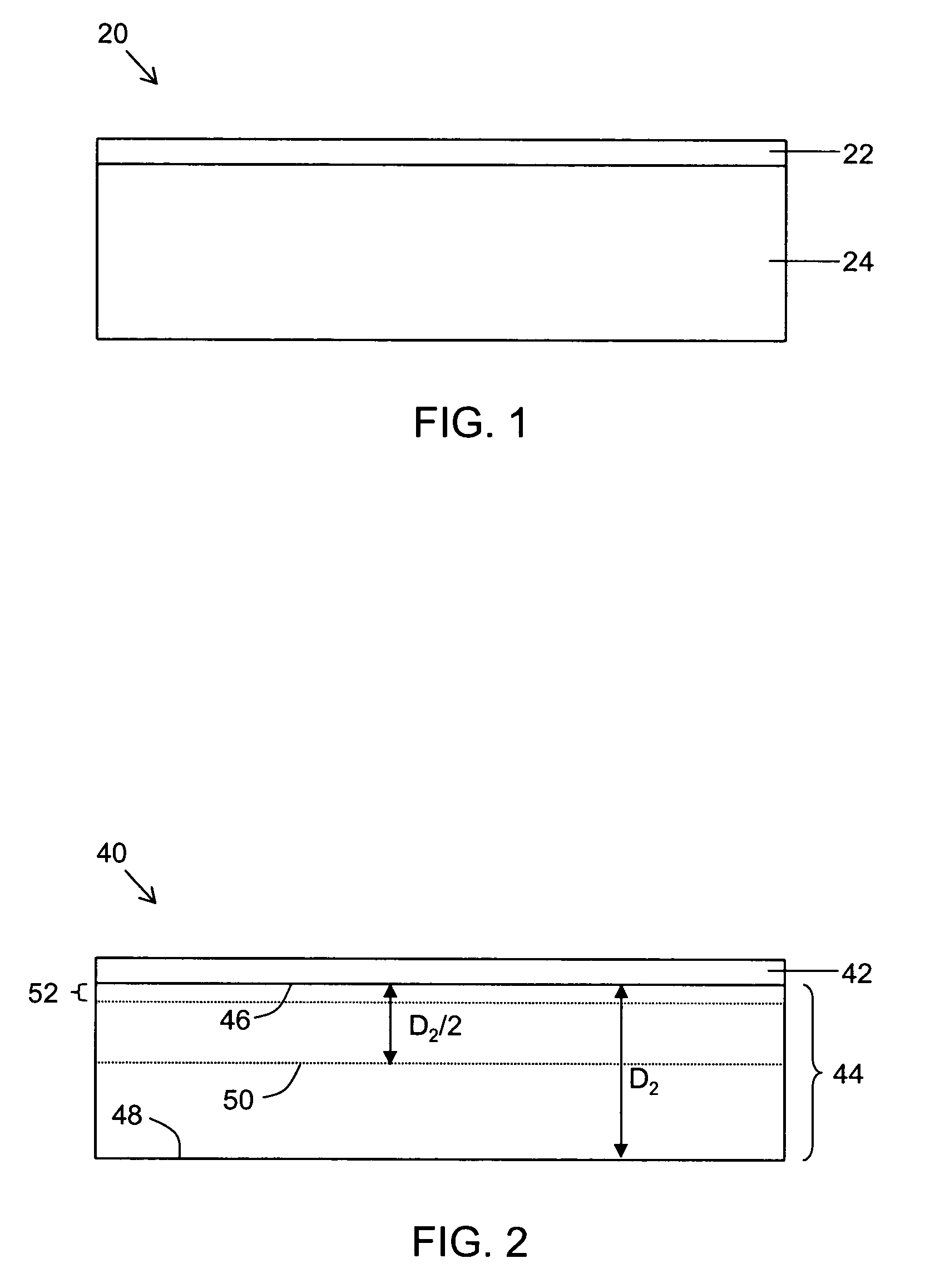
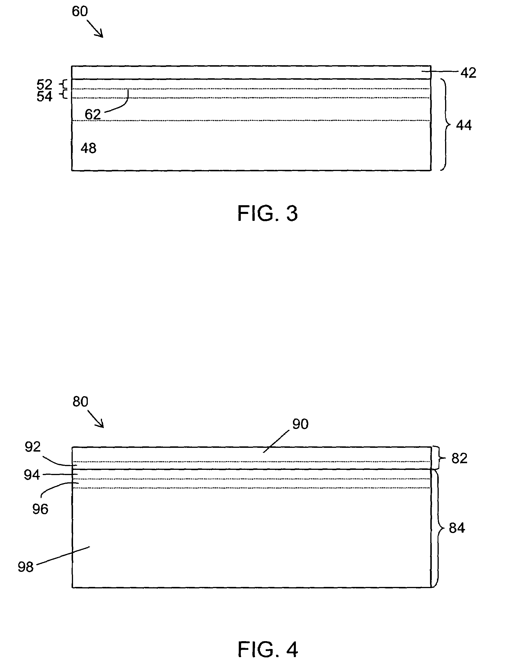
[0138]A 100 mm diameter, 1 mm thick wafer of glass 3N of Table 3 was polished to smoothness. A silicon wafer 525 μm in thickness was implanted with hydrogen at 100 keV and an ion dosage of 8×10¹⁶ ions / cm2 was cleaned with detergent and distilled water followed by a 10% nitric acid wash, and brought into contact with the glass wafer in a SUSS MICROTEC bonder. The glass wafer was heated at 450° C. and the silicon wafer at 400° C. in vacuum, and 10 psi pressure and 1750 V potential difference (glass at ground, silicon wafer at 1750 V) was applied for five minutes. While under the same potential difference and pressure, the glass wafer was heated at 575° C. and the silicon wafer at 525° C. for ten minutes, after which time the potential difference and pressure were removed, and the bonded wafers allowed to cool down. The cooled wafers separated into a silicon-on-glass wafer with a thin silicon layer, and a silicon wafer. The silicon layer on the glass had a thin, damaged top layer, and ...


PUM

PropertyMeasurementUnit
strain pointaaaaaaaaaa
thicknessaaaaaaaaaa
thicknessaaaaaaaaaa

Abstract

The present invention relates to semiconductor-on-insulator structures having strained semiconductor layers. According to one embodiment of the invention, a semiconductor-on-insulator structure has a first layer including a semiconductor material, attached to a second layer including a glass or glass-ceramic, with the CTEs of the semiconductor and glass or glass-ceramic selected such that the first layer is under tensile strain. The present invention also relates to methods for making strained semiconductor-on-insulator layers.

Description

[0001]This application claims priority from provisional application 60 / 602,782, filed Aug. 18, 2004.BACKGROUND OF THE INVENTION[0002]1. Field of the Invention[0003]The present invention relates generally to semiconductor structures, and more particularly to semiconductor-on-insulator structures and methods for making semiconductor-on-insulator structures.[0004]To date, the semiconductor material most commonly used in semiconductor-on-insulator structures has been silicon. Such structures have been referred to in the literature as silicon-on-insulator structures and the abbreviation “SOI” has been applied to such structures. The present invention relates to semiconductor-on-insulator structures in general, including silicon-on-insulator structures.[0005]For ease of presentation, the following discussion will at times be in terms of silicon-on-insulator structures. The references to this particular type of semiconductor-on-insulator structure are made to facilitate the explanation of ...

Claims


Application Information

Patent Timeline
Patent Type & Authority Patents(United States)
IPC IPC(8): H01L27/01
CPCH01L21/76254H01L27/12
Inventor AITKEN, BRUCE GARDINERGADKAREE, KISHOR PURUSHOTTAMDEJNEKA, MATTHEW JOHNPINCKNEY, LINDA RUTH
Owner CORNING INC
Why Eureka
Try Eureka