Check patentability & draft patents in minutes with Patsnap Eureka AI!

Refresh circuit for use in semiconductor memory device and operation method thereof

a technology of semiconductor memory devices and circuits, applied in the field of refresh circuits, can solve the problems of increasing the power consumption of refresh operations, and achieve the effect of increasing the refresh cycle time and reducing the peak curren

Active Publication Date: 2007-08-28
SK HYNIX INC
View PDF8 Cites 5 Cited by
  • Summary
  • Abstract
  • Description
  • Claims
  • Application Information

AI Technical Summary

Benefits of technology

The solution effectively reduces peak current required for refresh operations without increasing the refresh cycle time, thereby optimizing power consumption and operational efficiency.

Problems solved by technology

However, as the SDRAM is highly integrated, the number of memory cells connected to a single row address is increased and, thus, a power consumption for the refresh operation is increased.

Method used


Image

  • Refresh circuit for use in semiconductor memory device and operation method thereof
  • Refresh circuit for use in semiconductor memory device and operation method thereof
  • Refresh circuit for use in semiconductor memory device and operation method thereof

Examples


Embodiment Construction

[0015]Hereinafter, a refresh circuit in accordance with the present invention will be described in detail referring to the accompanying drawings.

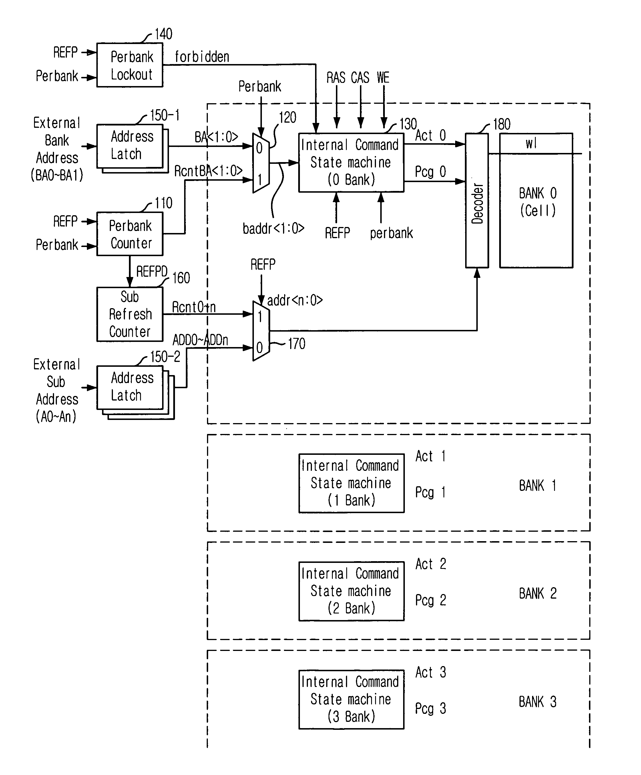
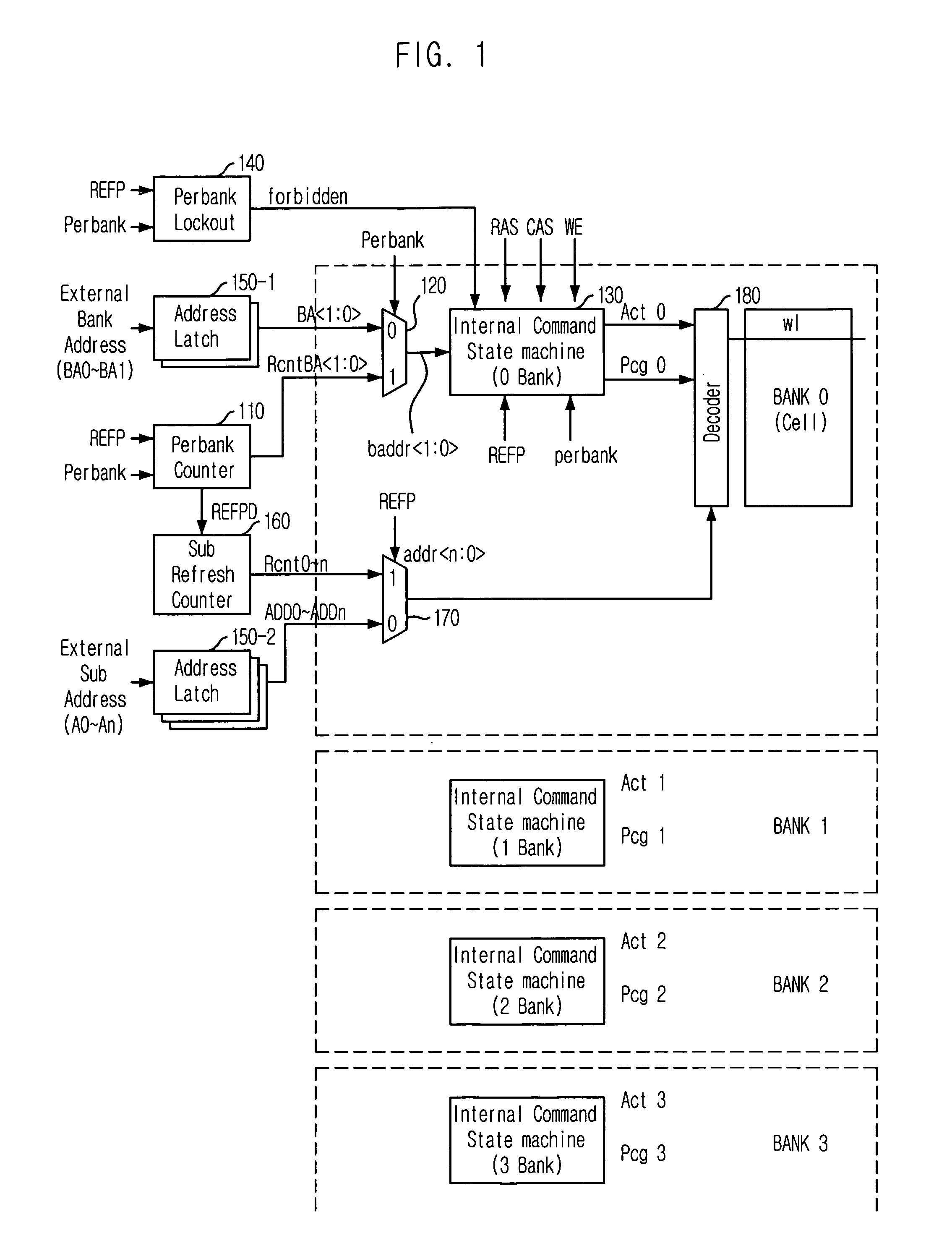
[0016]FIG. 1 is a block diagram showing a refresh circuit for individually refreshing banks included in a semiconductor memory device in accordance with a preferred embodiment of the present invention.

[0017]As shown, the refresh circuit includes a perbank counter 110, a perbank multiplexer 120, an internal command state machine 130 and a perbank lockout unit 140. Herein, it is assumed that the semiconductor memory device includes four banks.

[0018]At a normal operation mode, when an external address signal including an external bank address signal BA0:1> and an external sub address signal A0:n> is inputted, the perbank multiplexer 120 passes the external bank address signal BA0:1> in response to a perbank command Perbank and a sub multiplexer 170 passes the external sub address signal A0:n> in response to the perbank command Perbank.

[0019]A ...


PUM


Abstract

A refresh circuit for individually performing a refresh operation to a plurality of banks included in a semiconductor memory device, includes: a perbank counter for generating a refresh bank address according to a refresh pulse signal and a perbank command; a perbank multiplexer for selectively outputting one of the refresh bank address and a data access bank address in response to the perbank command; and an internal command state machine for generating a refresh command in response to the refresh pulse signal and the perbank command.

Description

FIELD OF INVENTION[0001]The present invention relates to a refresh circuit for use in a semiconductor memory device; and, more particularly, to a refresh circuit for individually performing a refresh operation to banks included in a semiconductor memory device.DESCRIPTION OF PRIOR ART[0002]Since a dynamic random access memory (DRAM) is a volatile memory device, the DRAM requires a refresh operation in order to hold a data stored in a memory cell. In case of a synchronous DRAM (SDRAM), a plurality of banks are included in the SDRAM and each bank includes memory cells in a matrix form corresponding to a row address and a column address. If each of four banks has 8K numbers of row addresses, four row addresses are activated for a single refresh operation. Accordingly, when 8K numbers of refresh operations are performed, the refresh operation is completed, i.e., all the memory cells are refreshed.[0003]However, as the SDRAM is highly integrated, the number of memory cells connected to a...

Claims


Application Information

Patent Timeline
Patent Type & Authority Patents(United States)
IPC IPC(8): G11C7/00
CPCG11C11/406G11C11/40618G11C8/12G11C11/4076G11C11/408
Inventor LEE, IHL-HO
Owner SK HYNIX INC
Features
  • R&D
  • Intellectual Property
  • Life Sciences
  • Materials
  • Tech Scout
  • Unparalleled Data Quality
  • Higher Quality Content
  • 60% Fewer Hallucinations
Learn More