Integrated circuit chip having non-volatile on-chip memories for providing programmable functions and features

a technology of integrated circuit chips and on-chip memories, which is applied in the direction of static storage, digital storage, instruments, etc., to achieve the effect of less die area, less expensive and complex

Active Publication Date: 2007-08-28
AVAGO TECH INT SALES PTE LTD
View PDF8 Cites 76 Cited by
  • Summary
  • Abstract
  • Description
  • Claims
  • Application Information

AI Technical Summary

Benefits of technology

[0010]The use of OTP memories in accordance with the present invention provides an advantage as compared to the use of metal fuses since OTP memories occupy less die area than metal fuses. Additionally, because blowing metal fuses require the use of a wafer probe, laser, or the like, this approach can only be used prior to packaging, whereas OTP memories can be programmed after packaging. Furthermore, since OTP memories can be implemented as part of the same standard fabrication processes used to manufacture the silicon chip, such as standard complementary metal oxide semiconductor (CMOS) processes, the use of OTP memories is considerably less expensive and complex as compared to the use of E2PROM technology, which requires additional processing steps.
[0013]In accordance with further embodiments of the present invention, one or more redundant OTP memory cells are advantageously used to achieve reprogrammability and / or to offset the possibility that one or more OTP memory cells are defective or otherwise non-functioning at the time of production of the integrated circuit chip. For example, by providing such redundancy, the integrated circuit chip manufacturer need not test each memory cell on a bit-by-bit basis as is often done for conventional E2PROMs, which is a complex and expensive process. Rather, the possibility of non-functioning OTP memory cells can be compensated for by simply providing a suitable number of redundant OTP memory cells.

Problems solved by technology

Additionally, because blowing metal fuses require the use of a wafer probe, laser, or the like, this approach can only be used prior to packaging, whereas OTP memories can be programmed after packaging.

Method used


Image

  • Integrated circuit chip having non-volatile on-chip memories for providing programmable functions and features
  • Integrated circuit chip having non-volatile on-chip memories for providing programmable functions and features
  • Integrated circuit chip having non-volatile on-chip memories for providing programmable functions and features

Examples


Embodiment Construction

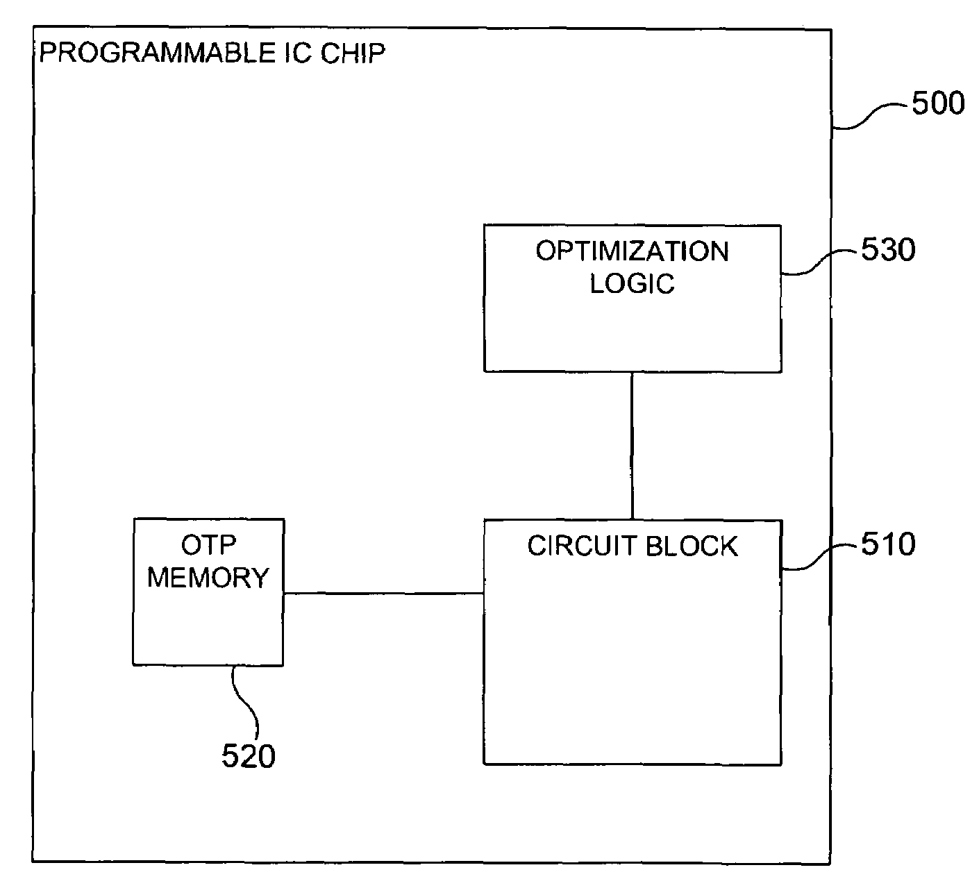
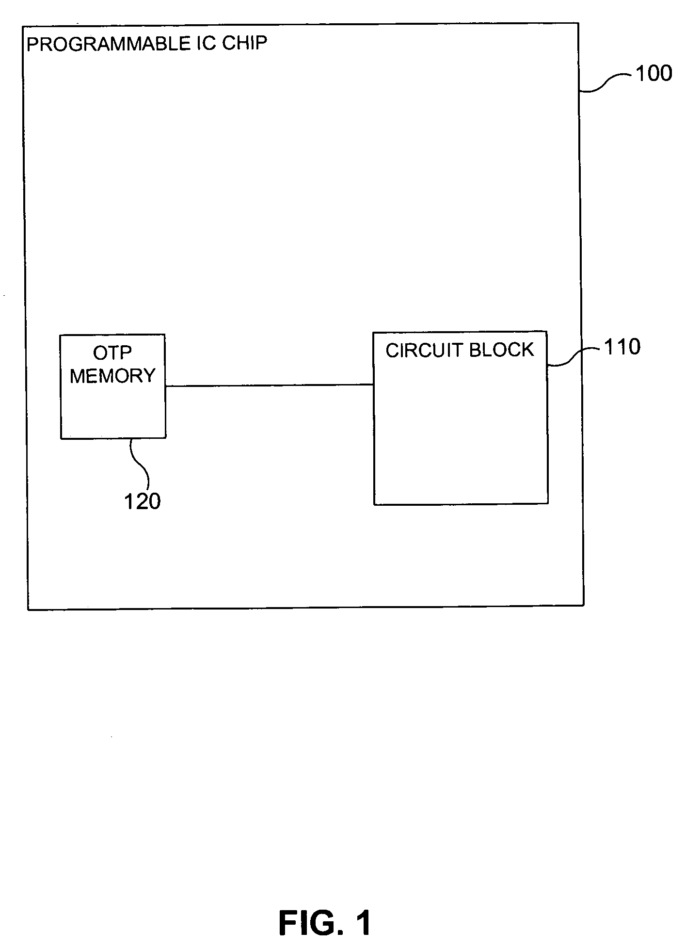
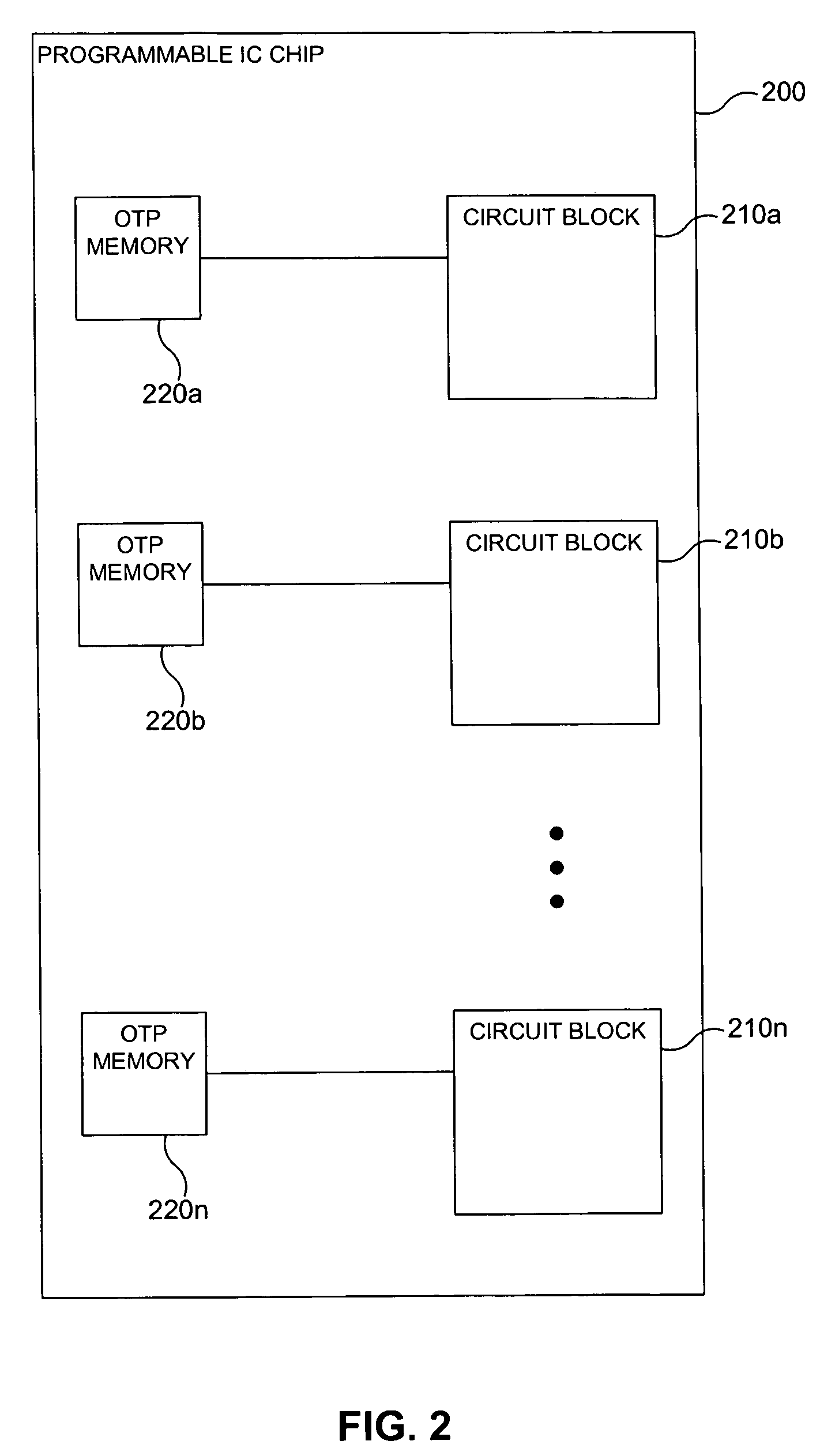
[0023]FIG. 1 illustrates a programmable integrated circuit chip 100 in accordance with an embodiment of the present invention. As shown in FIG. 1, programmable integrated circuit chip 100 includes a circuit block 110 coupled to an OTP memory 120.

[0024]Circuit block 110 comprises logic that is configured to perform one or more functions of programmable integrated circuit chip 100. As will be discussed in more detail herein, such functions may include, by way of example, providing a reference voltage or performing a power sequencing function. However, these examples are not intended to be limiting and a person skilled in the art will readily appreciate that numerous other functions may be performed by circuit block 100.

[0025]OTP memory 102 comprises one or more OTP memory cells. The OTP memory cells may be arranged as an array or as one or more banks of cells. Each OTP memory cell comprises a non-volatile storage element and a fuse element. The storage element may store either a logic...


PUM


Abstract

An integrated circuit chip having programmable functions and features in which one-time programmable (OTP) memories are used to implement a non-volatile memory function, and a method for providing the same. The OTP memories may be based on poly-fuses as well as gate-oxide fuses. Because OTP memories are small, less die area is utilized as compared to metal fuses. Addtionally, because OTP memories can be implemented as part of standard complementary metal oxide semiconductor (CMOS) processes, the method is less costly and complex than the use of electrically-erasable programmable read-only memories (E2PROMs).

Description

CROSS REFERENCE TO RELATED APPLICATIONS[0001]This application claims the benefit of U.S. Provisional Application No. 60 / 618,258, filed Oct. 14, 2004, which is incorporated by reference herein.BACKGROUND OF THE INVENTION[0002]1. Field of the Invention[0003]The present invention is generally directed to integrated circuit chips having programmable functions and features.[0004]2. Background[0005]It is often desirable to be able to alter the functions and features of an integrated circuit chip during and / or after manufacturing thereof. In order to do so, the chip can be designed in a way such that those features can be programmed using on-chip memory. Conventionally, the on-chip memory required for such programmability has been implemented through, for example, metal fuses and / or electrically-erasable programmable read-only memories (E2PROMs).[0006]Metal fuses have been used, for example, to allow trimming of accurate voltage reference sources in silicon chips. Metal fuses usually occup...

Claims


Application Information

Patent Timeline
Patent Type & Authority Patents(United States)
IPC IPC(8): G11C17/18G11C7/00
CPCG11C17/16
Inventor KIM, NEIL Y.VORENKAMP, PIETER
Owner AVAGO TECH INT SALES PTE LTD
Why Eureka
Try Eureka