Method of driving electron-emitting device, electron source, and image-forming apparatus

a technology of electron-emitting device and electron source, which is applied in the manufacture of electrode systems, instruments, electric discharge tubes/lamps, etc., can solve the problems of variation or deterioration of electron-emitting characteristics, and achieve the effects of improving stability, reproducing high, and prolonging li

Inactive Publication Date: 2007-09-04
CANON KK
View PDF45 Cites 8 Cited by
  • Summary
  • Abstract
  • Description
  • Claims
  • Application Information

AI Technical Summary

Benefits of technology

[0021]An object of the present invention is to provide a manufacturing method capable of manufacturing a surface conduction electron-emitting device using a specific substrate on which a film containing silicon oxide (such as SiO2) as a main component is provided, in which a variation in device current If at the time of manufacturing is suppressed and thus uniformity of the device current If is high. Another object of the present invention is to provide a method of manufacturing an electron source using the electron-emitting device and a method of manufacturing an image display apparatus using the electron-emitting device. Still another object of the present invention is to provide a driving method of realizing a uniform electron-emitting characteristic in each of the electron-emitting device, the electron source, and the image display apparatus.
[0035]According to the present invention, the device current If based on the applied pulse voltage can be observed with high reproductivity. Accordingly, it is possible to correctly set a value of the pulse voltage applied to obtain a desirable device current If. Therefore, a uniform electron-emitting region can be formed. As a result, it is possible to provide an electron-emitting device whose life is lengthened and stability is improved and in which a variation in device characteristic is reduced, an electron source using the electron-emitting device, and an image display apparatus using the electron-emitting device. According to a driving method of the present invention, the stable and uniform electron emission is realized, so that a high quality image can be displayed.

Problems solved by technology

As a result, such a substrate causes a variation or deterioration in electron-emitting characteristic.
However, it was found that a surface conduction electron-emitting device using the glass substrate which contains silicon oxide as a main ingredient, Na2O, and K2O, in which the molar ratio of K2O to Na2O is 0.5 to 2.0, and has the film containing SiO2 as a main component provided on its surface may have the following problem.

Method used


Image

  • Method of driving electron-emitting device, electron source, and image-forming apparatus
  • Method of driving electron-emitting device, electron source, and image-forming apparatus
  • Method of driving electron-emitting device, electron source, and image-forming apparatus

Examples


embodiments

(First Embodiment)

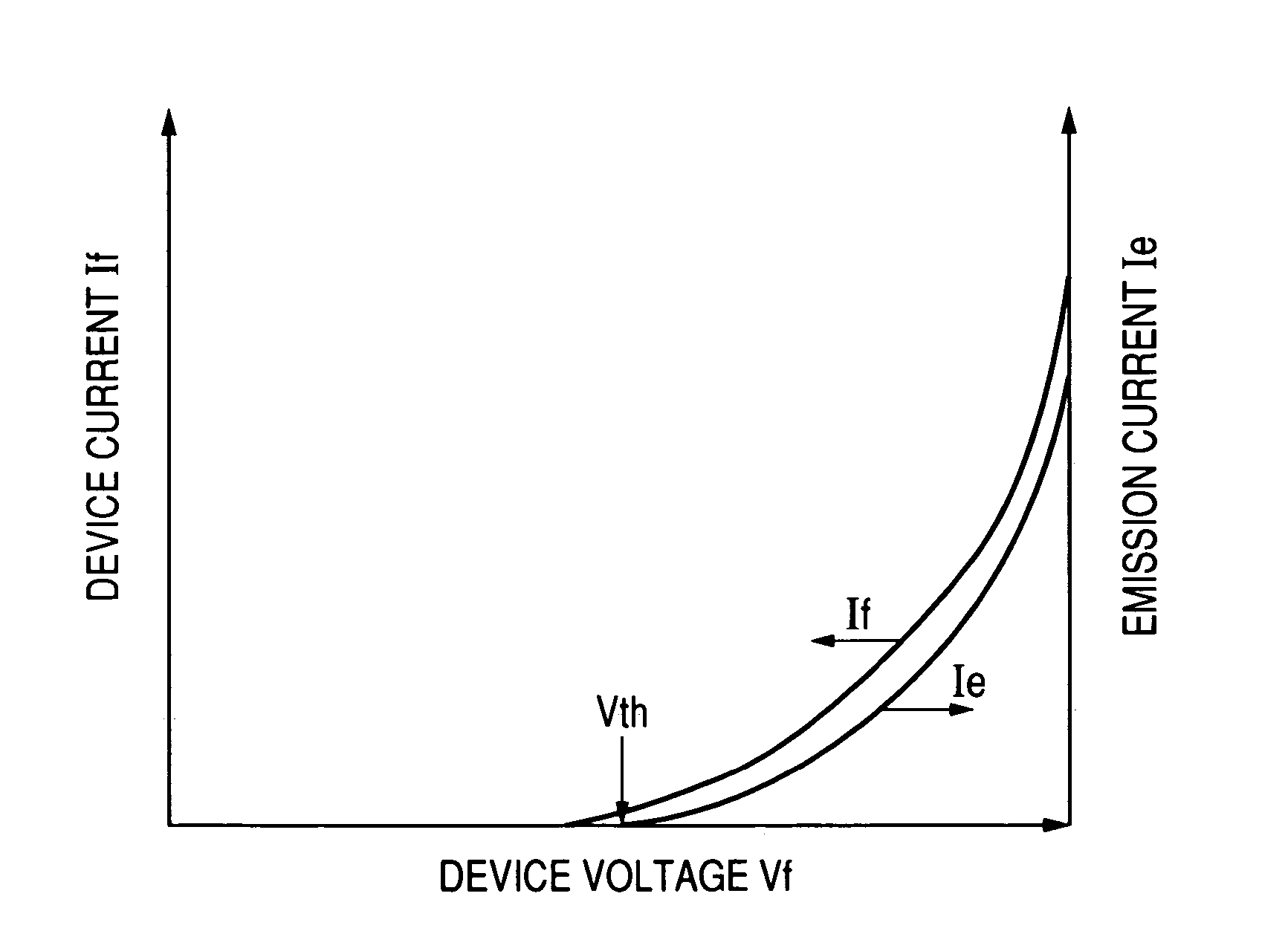
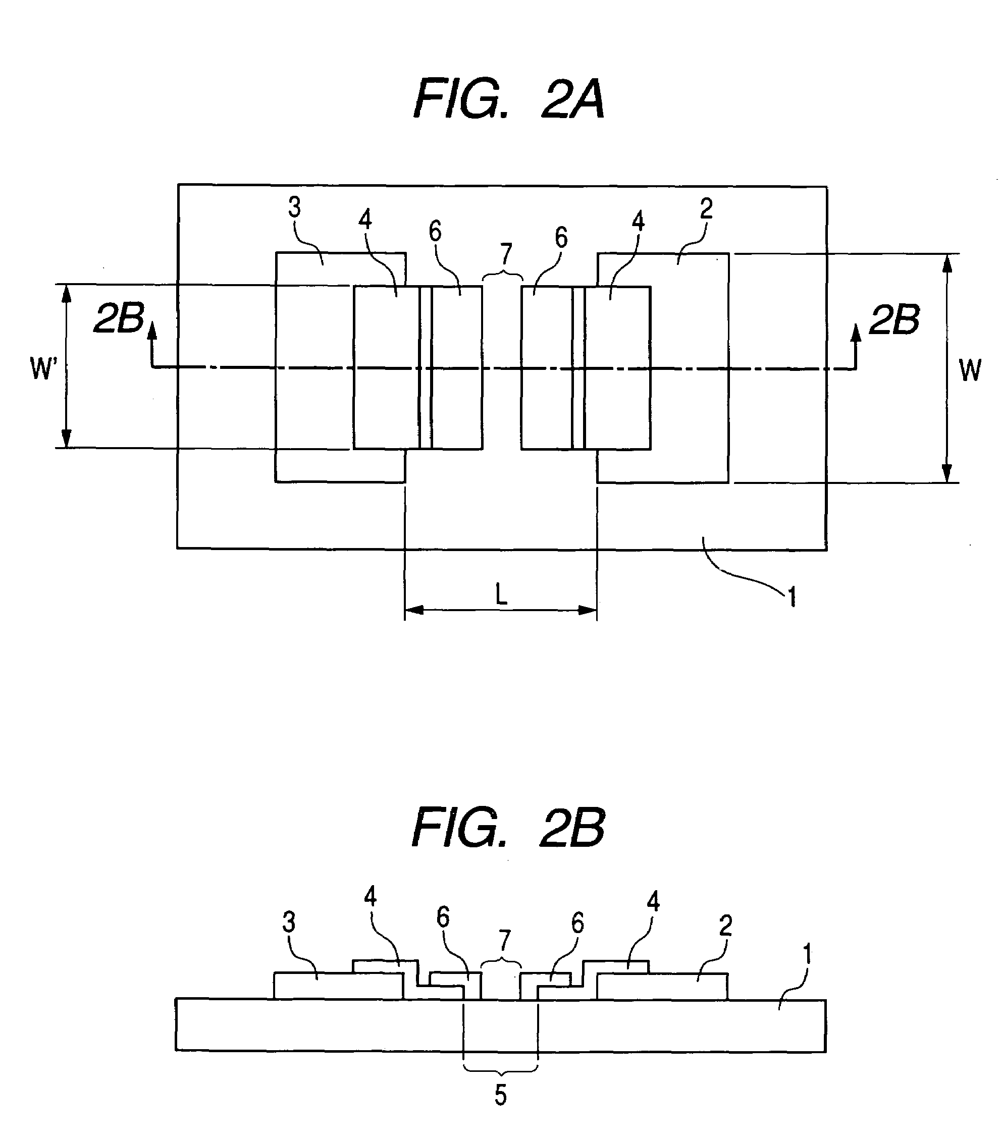
[0108]In a first embodiment, the electron-emitting device having the structure shown in FIGS. 2A and 2B is manufactured. FIG. 2A is a plan view showing the electron-emitting device. FIG. 2B is a cross sectional view along the line 2B-2B in FIG. 2A. In FIGS. 2A and 2B, reference numeral 1 denotes a substrate, 2 and 3 denote the electrodes (set of electrodes), 4 denotes electroconductive films, 5 denotes a second gap, 6 denotes a carbon film, and 7 denotes a first gap.

[0109]In this embodiment, five electron-emitting devices are manufactured according to the following steps.

[0110]Step (a)

[0111]Used here is the substrate 1 composed of a glass substrate and a film which covers the glass substrate and contains SiO2 as a main component. The glass substrate contains 67% of SiO2, 4.4% of K2O, and 4.5% of Na2O in terms of molar ratio. A strain point of the glass substrate is 570° C. The film containing SiO2 as a main component is formed at a thickness of about 380 nm on the ...

second embodiment

[0148]In a second embodiment, the substrate 1 composed of a glass substrate and a film containing SiO2 as a main component is used instead of the substrate 1 in the first embodiment. The glass substrate contains 66% of SiO2, 5.4% of K2O, and 5.0% of Na2O in terms of molar ratio and has a strain point of 582° C. The film is formed at a thickness of 380 nm on the glass substrate by a sputtering evaporation method. Steps up to step (g) are performed as in the first embodiment. Even in this embodiment, five electron-emitting devices “A” to “E” are manufactured as in the first embodiment.

[0149]As in the first embodiment, the stabilization step corresponding to step (g) is performed and then the electron-emitting characteristic measurement corresponding to step (h) is performed.

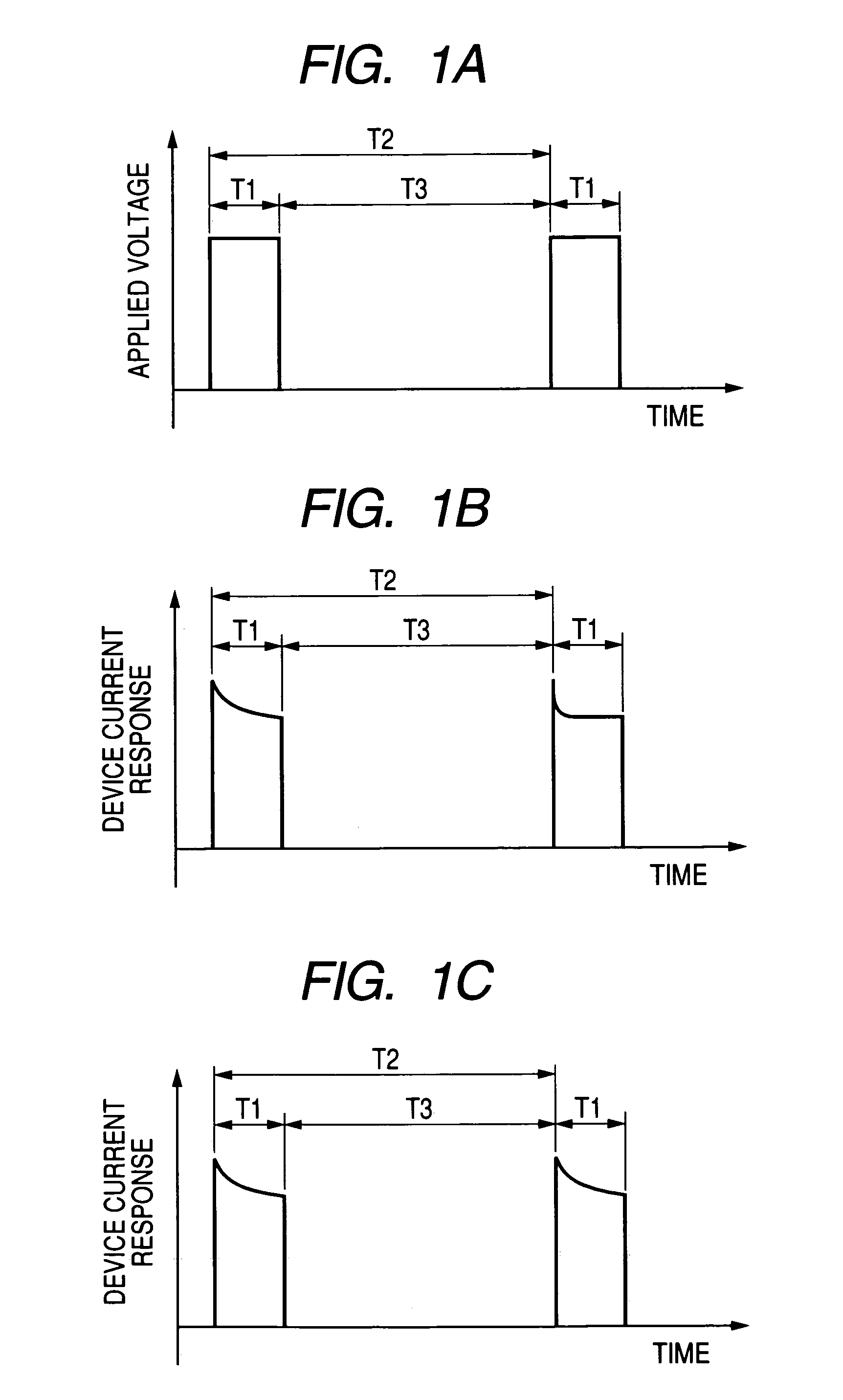
[0150]First, a single electron-emitting device “A” of the five electron-emitting devices is used and the pulse voltage shown in FIG. 1A is applied between the electrodes 2 and 3. More specifically, a waveform whose...

third embodiment

[0167]In a third embodiment, used is a substrate in which the film containing SiO2 as a main component is formed at the thickness of about 380 nm on the glass substrate which contains 67% of SiO2, 4.4% of K2O, and 4.5% of Na2O in terms of molar ratio as used in the first embodiment by a sputtering evaporation method. In this embodiment, a single electron-emitting device is manufactured.

[0168]In this embodiment, a resistor of 300 Ω is inserted between the electrode 2 and the power source for pulse voltage application. This assumes the case where a plurality of electron-emitting devices are connected in parallel, providing a state in which a pulse voltage is significantly influenced by voltage drop caused by wirings and the like which are located between the power source for pulse voltage application and the electrodes when a large device current flows.

[0169]For example, when the device current If is changed with the progress of the activation step, the voltage drop expressed by a pro...


PUM


Abstract

Provided is a manufacturing method capable of manufacturing an electron-emitting device in which a variation in device current at the time of manufacturing is suppressed and thus uniformity thereof is high. The electron-emitting device includes a substrate, a first conductor, and a second conductor. The substrate is composed of: a member which contains silicon oxide as a main ingredient, Na2O, and K2O and in which a molar ratio of K2O to Na2O is 0.5 to 2.0; and a film which contains silicon oxide as a main component and is stacked on the member. The first conductor and the second conductor are located on the substrate. In a forming step and / or an activation step, a quiescent period (interval) of a pulse voltage applying repeatedly applied between the first conductor and the second conductor is set equal to or longer than 10 msec.

Description

BACKGROUND OF THE INVENTION[0001]1. Field of the Invention[0002]The present invention relates to an electron-emitting device, an electron source, and an image-forming apparatus, and a method of driving the same.[0003]2. Related Background Art[0004]Surface conduction electron-emitting device is known as one of an electron-emitting device. A method of manufacturing the surface conduction electron-emitting device is disclosed in, Japanese Patent Application Laid-Open Nos. H08-264112, H08-321254, H10-228867, 2000-306500, 2001-319564, H01-279538, 2000-243225, H09-265900, 2000-311593, and 2000-030605. According to this manufacturing method, a “forming step” for forming a gap in a portion of an electroconductive film is performed. If necessary, a treatment called an “activation step” is further performed.[0005]The “activation step” can be performed by repeatedly applying a pulse voltage to the electroconductive film on which the “forming step” has been completed in an atmosphere including ...

Claims


Application Information

Patent Timeline
Patent Type & Authority Patents(United States)
IPC IPC(8): H01J9/02H01J9/00H01J9/42G09G3/10G09G3/20G09G3/22
CPCG09G3/22H01J29/863H01J31/127H01J2329/0489H01J2329/8615
Inventor KOBAYASHI, TAMAKIYAMAMOTO, KEISUKE
Owner CANON KK
Why Eureka
Try Eureka