Open loop bandwidth test architecture and method for phase locked loop (PLL)

a bandwidth test and open-loop technology, applied in the field of electronic circuits, can solve the problems of slow approach, inefficient, expensive, and complex methods that cannot be achieved, and achieve the effect of easy testing

Active Publication Date: 2007-09-04
MONTEREY RES LLC
View PDF31 Cites 58 Cited by
  • Summary
  • Abstract
  • Description
  • Claims
  • Application Information

AI Technical Summary

Benefits of technology

[0021]According to another aspect of the embodiments, a PLL circuit can further include a phase detector circuit that provides a phase difference value. In a test mode, the phase difference value can vary according to test input values. In a non-test mode, the phase difference value can be based a difference between an input signal and feedback signal. A charge pump circuit can be coupled to the control node and provide a current to the control node based on the phase difference value output from the phase detector circuit. In this way, different control voltages can be generated based on a test values provided to a phase detector circuit.
[0022]According to another aspect of the embodiments, a PLL circuit can further include a phase detector that generates a phase different value based on a phase difference between an input signal and a feedback signal. A charge pump can be coupled between the phase detector and control node that provides a current to the control node based on the phase difference value. In addition, a feedback path can be coupled between an output of the VCO and an input of the phase detector. The feedback path can include a loop switch that opens the feedback path in the test mode and remains closed in a non-test mode. In this way, different control voltages can be generated based on opening a feedback path of the PLL circuit.
[0023]According to another aspect of the embodiments, the loop filter is formed in the same integrated circuit substrate as other portions of the PLL. In such an arrangement, a PLL manufactured as an integrated or as a portion of an integrated circuit can be easily tested for an open loop bandwidth value.
[0024]The present invention can also include a method of testing a PLL circuit. The method can include enabling a test leg that draws current through a load resistance of a PLL loop filter to generate a control voltage at an input of a voltage controlled oscillator. The method can also include varying the control voltage and measuring the output frequency of the PLL for each of the different control voltages. Such a method can help arrive at an open loop bandwidth determination for a PLL without invasive or time consuming testing.

Problems solved by technology

Such methods present a more complex or invasive method than could be achieved through automated chip / part testing.
As result, such approaches can be slow, inefficient, and expensive.

Method used


Image

  • Open loop bandwidth test architecture and method for phase locked loop (PLL)
  • Open loop bandwidth test architecture and method for phase locked loop (PLL)
  • Open loop bandwidth test architecture and method for phase locked loop (PLL)

Examples


first embodiment

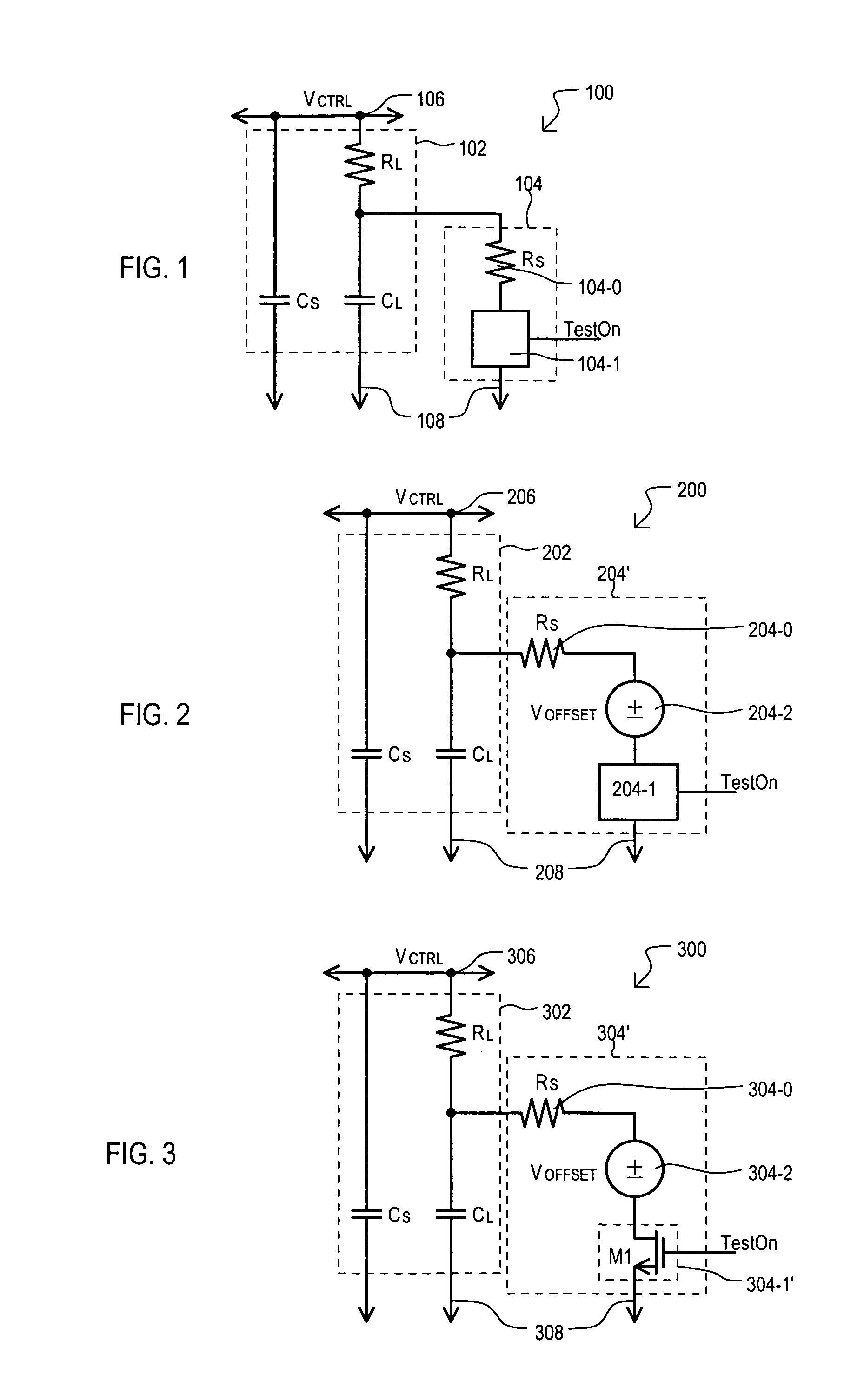
[0043]the present invention can include a test loop filter of a PLL circuit. A test loop filter is designated by the general reference character 100, and can include a resistor-capacitor (RC) network 102 and a test leg 104. An RC network 102 can be situated between a control node 106 and a supply node 108 (in this case a low voltage power supply node, such as ground). In the very particular example of FIG. 1, RC network 102 can include a load resistance RL, a first capacitor CL, and a second capacitor CS. A load resistance RL can be connected in series with first capacitor CL between a control node 106 and supply node 108. A second capacitor CS can be connected in parallel with load resistor RL and first capacitor CL between control node 106 and supply node 108.

[0044]A test leg 104 can be connected to a load resistance RL, and when enabled, can provide a current path through load resistance RL. In the very particular example shown in FIG. 1, a test leg 104 can include a test resista...

fourth embodiment

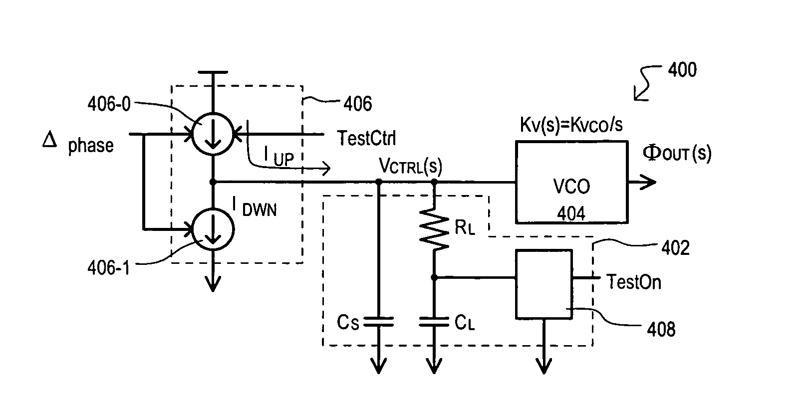
[0054]FIG. 4 shows a block schematic diagram of a PLL circuit section according to a A PLL circuit section is designated by the general reference character 400 can include a test loop filter 402, voltage controlled oscillator (VCO) 404, and charge pump circuit 406. A test loop filter 402 can take the form of any of the above embodiments or equivalents, and can provide a control voltage VCTRL that depends upon a current provided to loop filter 402 from charge pump circuit 406. A VCO 404 can generate an output signal ΦOUT having a frequency that depends upon control voltage VCTRL.

[0055]FIG. 4 illustrates a case in which a current IUP provided to a test loop filter 402 during a test can be generated by additional current switching in the charge pump 404. More particularly, a charge pump 404 may provide a current IUP from a controllable current source 406-0 to a loop filter 402 according to test value TestCtrl.

[0056]In a non-test mode, current IUP can be based on a phase difference val...

fifth embodiment

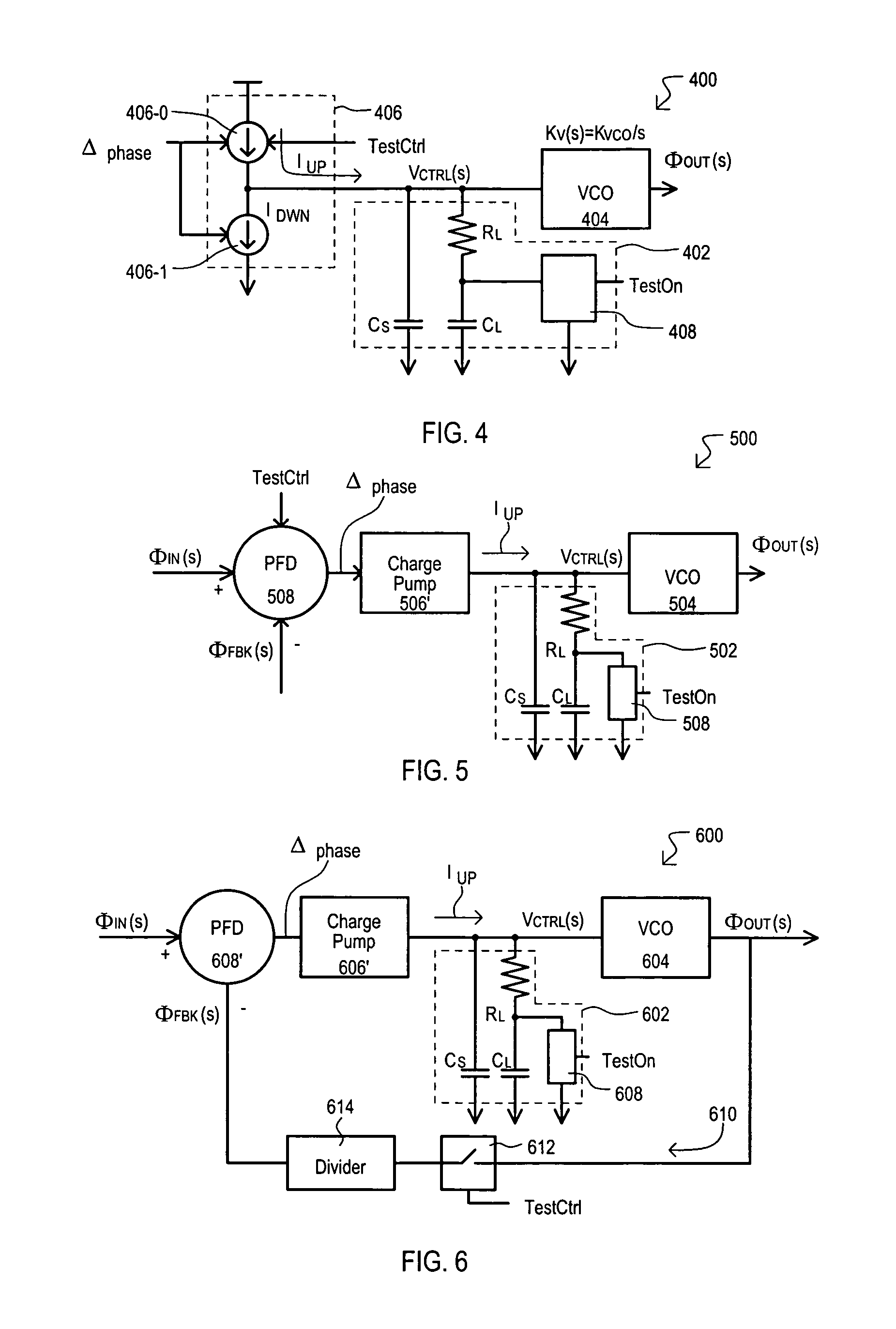
[0060]FIG. 5 shows a block schematic diagram of a PLL circuit section according to a A PLL circuit section is designated by the general reference character 500 can include some of the same general components as the embodiment of FIG. 4. Thus, like components are referred to by the same reference character but with the first digit begin a “5” instead of a “4”.

[0061]A PLL circuit section 500 can differ from that of FIG. 4 in that a charge pump 506′ can be conventional in design, and not provide additional current switching in a test mode. Further, a PLL circuit section 500 can also include an adjustable phase detector (PFD) 508. An adjustable PFD 508 can include additional logic over a conventional PFD that enables the adjustable PFD 508 to generate a phase difference value that does not only depend upon a difference between an input signal and feedback signal.

[0062]In a non-test mode, a phase difference value Δphase can be generated by a PDF 508 based on a phase difference between a...


PUM


Abstract

A phase locked loop (PLL) can include a test loop filter (100) that generates a control voltage (VCTRL) for input to a voltage controlled oscillator (VCO). In a test mode, a control voltage can be varied and resulting output frequencies recorded, from which an open loop bandwidth can be determined. A control voltage can be varied by enabling a switch element (104-1) that can provide a current path through load resistance (RL) of test loop filter (100). Current provided to the test loop filter can be varied according to test signals to provide a variable control voltage (VCTRL).

Description

[0001]This application claims the benefit of U.S. Provisional Patent Application Ser. No. 60 / 579,944 filed on Jun. 14, 2004, the contents of which are incorporated by reference herein.TECHNICAL FIELD[0002]The present invention relates generally to electronic circuits, and more particularly to circuits that generate timing signals.BACKGROUND OF THE INVENTION[0003]In electronic systems, timing signals can be very important to the overall performance of the system. One widely used way to synchronize operations of a system (e.g., integrated circuit) with an externally received clock can be with a phase locked loop (PLL). PLLs can address many common timing problems associated with generating a clock signal, including but not limited to, unwanted clock skew and jitter. Of course, PLLs are widely in used in applications other than frequency synchronization, including but not limited to frequency synthesis, frequency translation, frequency detection, and frequency modulation.[0004]To bette...

Claims


Application Information

Patent Timeline
Patent Type & Authority Patents(United States)
IPC IPC(8): H03L7/00G01R23/00
CPCH03L7/0891H03L7/093
Inventor STIFF, JONATHON
Owner MONTEREY RES LLC
Why Eureka
Try Eureka