

Thick film electrode and multilayer ceramic electronic device
a multi-layer ceramic and thick film technology, applied in the direction of stacked capacitors, generators/motors, fixed capacitor details, etc., can solve the problems of fracturing the external electrode, multi-layer ceramic electronic devices do not function as electronic devices, and ceramic laminates, etc., to achieve poor electrical continuity, reduce conductivity, and improve durability and moisture resistance.
- Summary
- Abstract
- Description
- Claims
- Application Information
AI Technical Summary
Benefits of technology
Problems solved by technology
Method used
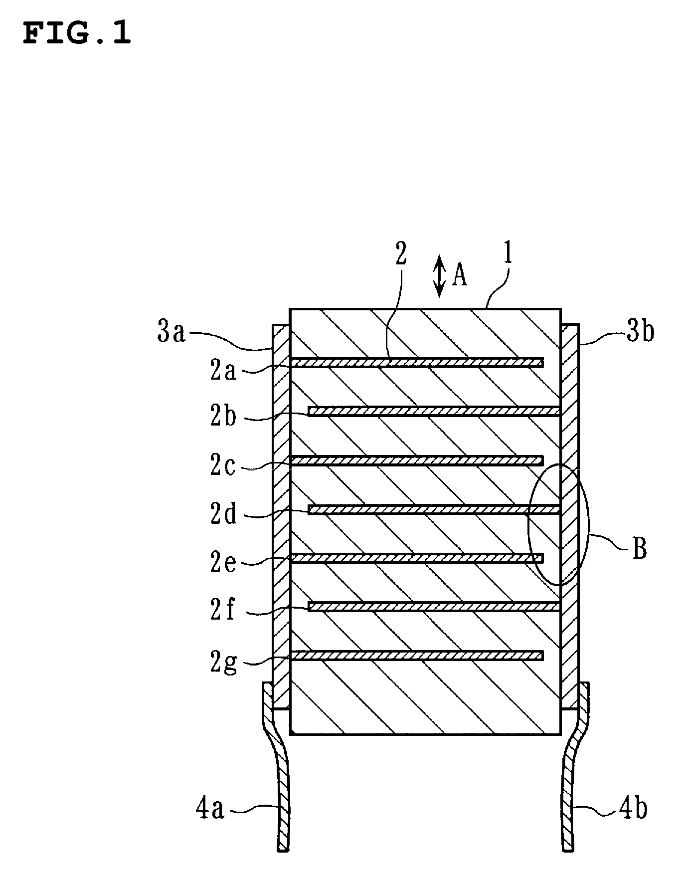
Image

Examples
example 1
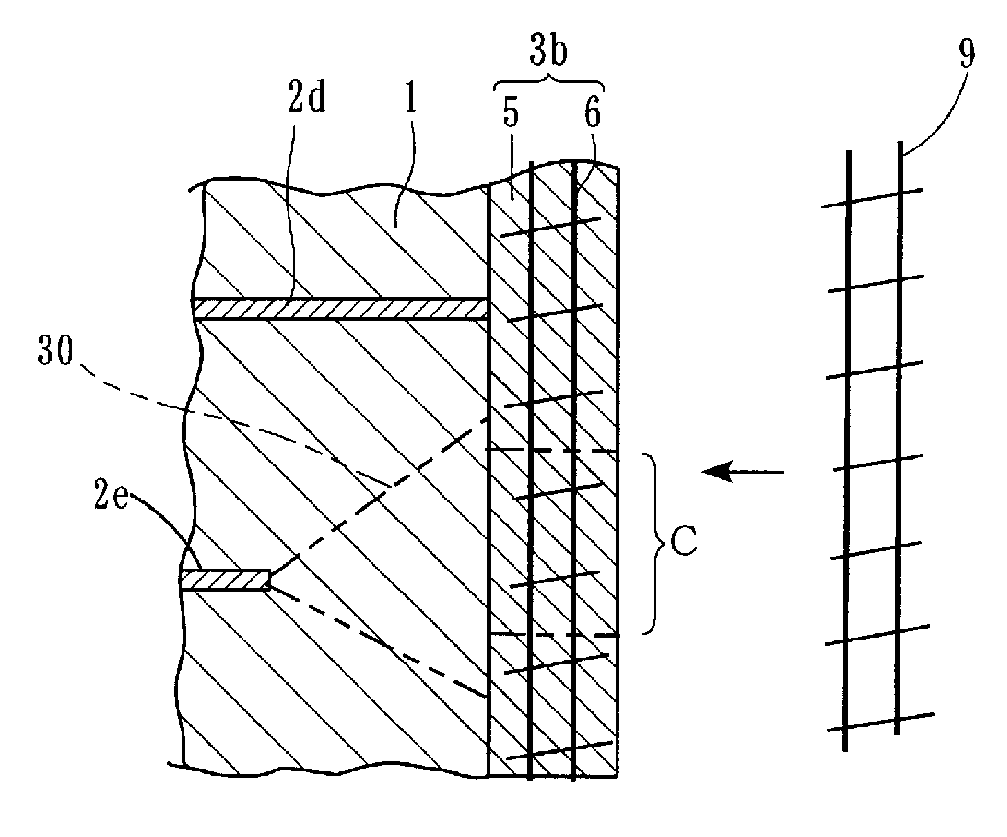
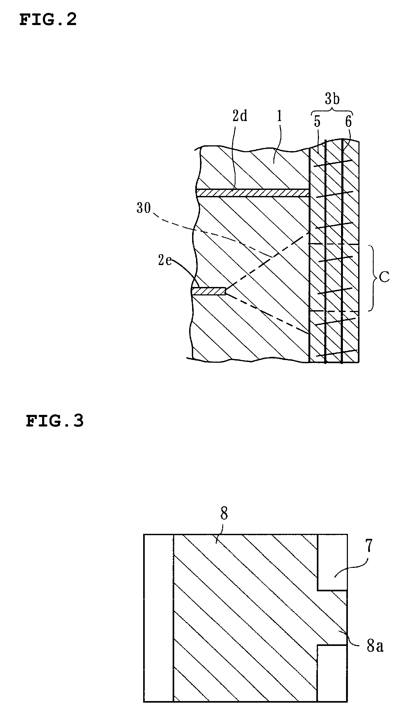
[0072]A conductive paste was prepared, the conductive paste being formed of an organic vehicle including about 50 to about 60 percent by weight of a Ag powder having an average particle size of about 2.0 μm, about 0.1 to about 7 percent by weight of glass frit, and an ethyl cellulose resin (binder resin) and butyl carbitol (organic solvent) constituting the remainder. The conductive paste is applied to both side surfaces of a multilayer piezoelectric body, including internal electrodes and having a length of about 7 mm, a width of about 7 mm, and a thickness of about 30 mm, by printing with a metal mask to form coating films each having a width of about 4 mm and a thickness of about 400 μm at both side surfaces of the multilayer piezoelectric body. An Ni grid having a wire diameter of about 100 μm and a mesh opening of 100 mesh was embedded in each coating film, dried at about 150° C. for about 10 minutes in an oven, and fired at about 740° C. in an air atmosphere to produce an exte...
example 2
[0074]External electrodes in which Ag grids were completely embedded in both side surfaces of the multilayer piezoelectric device to form a unitary structure were formed in the same process and procedure as those in Example 1, except that the Ag grids each having a wire diameter of about 100 μm and a mesh opening of 100 mesh were used in place of the Ni grids. After the connection of leads, piezoelectric properties were imparted, thereby producing a sample of Example 2.
example 3
[0075]The same Ni grids as those used in Example 1 were electrolytically plated with Ag to produce Ni grids covered with Ag films each having a thickness of about 30 μm.
[0076]Then, external electrodes in which the Ag-plated Ni grids were embedded in both side surfaces of a multilayer piezoelectric device to form a unitary structure were formed in the same process and procedure as those in Example 1. After leads were connected to the external electrodes, piezoelectric properties were imparted, thereby producing a sample of Example 3.
PUM
| Property | Measurement | Unit |
|---|---|---|
| temperature | aaaaa | aaaaa |
| temperature | aaaaa | aaaaa |
| thickness | aaaaa | aaaaa |
Abstract
Description
Claims
Application Information