Semiconductor device incorporating a semiconductor constructing body and an interconnecting layer which is connected to a ground layer via a vertical conducting portion

a technology of semiconductor constructing body and semiconductor, which is applied in the direction of semiconductor devices, solid-state devices, basic electric elements, etc., can solve the problems of increasing difficult alignment with the circuit board, and the inability to fabricate a csp in which the number of external connection electrodes is large, etc., and achieve suppressed deterioration of circuit characteristics

Inactive Publication Date: 2007-10-09
CMK
View PDF8 Cites 144 Cited by
  • Summary
  • Abstract
  • Description
  • Claims
  • Application Information

AI Technical Summary

Benefits of technology

[0011]It is, therefore, an object of the present invention to provide a novel semiconductor device by which the size and pitch of external connection electrodes can be set to a necessary size and pitch even if the number of these electrodes increases, an electronic apparatus can be further downsized, and deterioration of the circuit characteristics can be suppressed by minimizing the wiring length, and to provide a method of fabricating this semiconductor device.
[0019]In the present invention, the upper interconnections are formed on the semiconductor constructing body and on the insulating layer formed around the semiconductor constructing body. Therefore, even if the number of connecting pad portions (external connection electrodes) of the upper interconnections increases, the size and pitch of these connecting pad portions can be set to a necessary size and pitch. Also, that portion of the base member, which functions as a ground layer and the upper interconnection for grounding are connected via the vertical conducting portion formed in a through hole which is formed in at least the insulating layer. This makes it possible to further downsize the electronic apparatus, and improve the circuit characteristics by minimizing the wiring length.

Problems solved by technology

With this increase in integration degree of semiconductor devices, the number of external connection electrodes increases, and this poses the following problems.
This makes it impossible to fabricate a CSP in which the number of external connection electrodes is large compared to the size of a bare semiconductor device.
That is, if the size and pitch of external connection electrodes extremely decrease, alignment with a circuit board becomes difficult.
This also poses fatal problems that, e.g., the junction strength becomes insufficient, the external connection electrodes shortcircuit during bonding, and the electrodes are destroyed by stress produced by the difference between the linear thermal expansion of the semiconductor substrate which is usually a silicon substrate and that of the circuit board.
Therefore, the electronic apparatus can be greatly downsized compared to the face up bonding method using conventional wire bonding or the like, but this downsizing is still limited.
Since this poses a problem such as an increase of the impedance (e.g., stray capacitance), the circuit characteristics deteriorate in some cases.

Method used


Image

  • Semiconductor device incorporating a semiconductor constructing body and an interconnecting layer which is connected to a ground layer via a vertical conducting portion
  • Semiconductor device incorporating a semiconductor constructing body and an interconnecting layer which is connected to a ground layer via a vertical conducting portion
  • Semiconductor device incorporating a semiconductor constructing body and an interconnecting layer which is connected to a ground layer via a vertical conducting portion

Examples


first embodiment

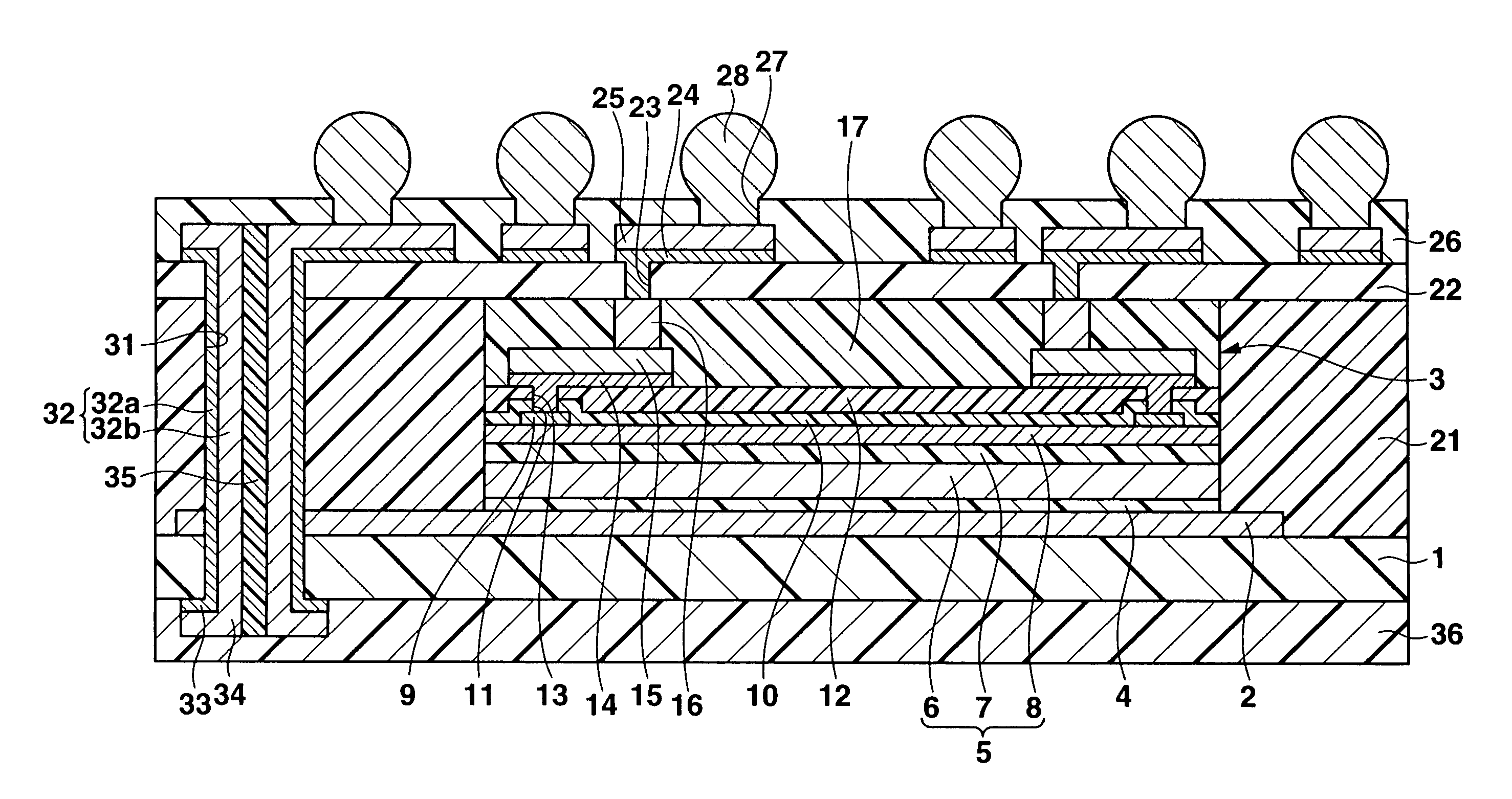
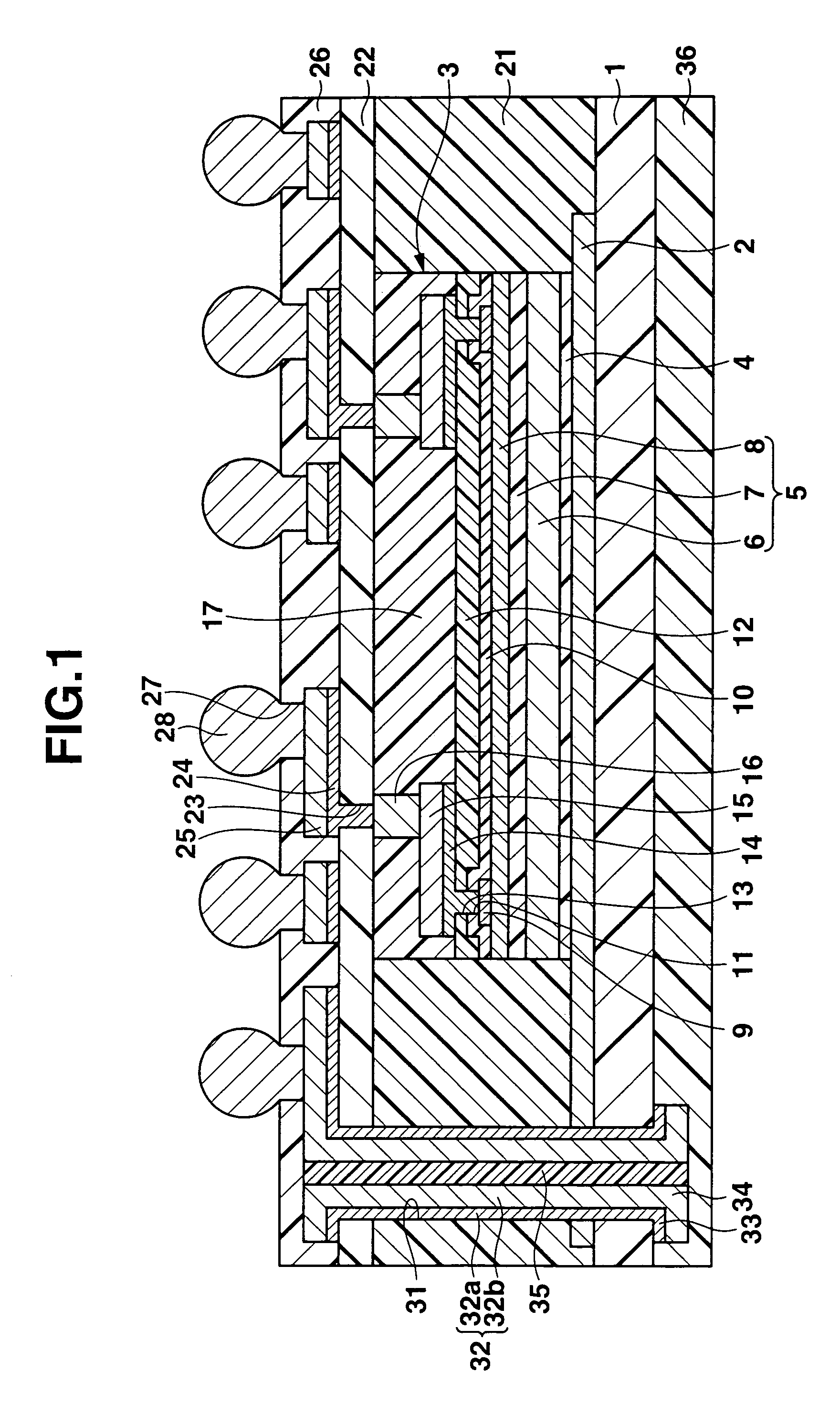
[0046]FIG. 1 is a sectional view of a semiconductor device as the first embodiment of the present invention. The semiconductor device has a base plate 1 made of an insulating material such as glass-fabric-base epoxy resin, and having a rectangular planar shape. A ground layer (metal foil) 2 made of copper foil and having a solid pattern is formed on the upper surface of the base plate 1. The base plate 1 and the ground layer 2 formed on the base plate 1 form a base member having the function of a ground layer.

[0047]The lower surface of a semiconductor constructing body 3 having a rectangular planar shape of a size somewhat smaller than the size of the base plate 1 is adhered to the upper surface of the ground layer 2 via an adhesive layer 4 made of a die bonding material. The semiconductor constructing body 3 has interconnections, columnar electrodes, and a sealing film (all of which will be described later), and is generally called a CSP. The semiconductor constructing body 3 is pa...

second embodiment

[0082]FIG. 16 is a sectional view of a semiconductor device as the second embodiment of the present invention. This semiconductor device differs from the semiconductor device shown in FIG. 1 in that a ground layer 2 is not directly connected to a vertical conducting portion 32, and a lower interconnection 34 including a lower metal undercoating 33 formed on the lower surface of a base plate 1 and connected to the vertical conducting portion 32 is connected to the lower surface of the ground layer 2 via a through hole 61 formed in the base plate 1. In this structure, the through hole 61 is formed in the base plate 1 made of, e.g., glass-fiber-base epoxy resin by laser processing which radiates a laser beam.

third embodiment

[0083]FIG. 17 is a sectional view of a semiconductor device as the third embodiment of the present invention. This semiconductor device differs from the semiconductor device shown in FIG. 1 in that a ground layer 2 is formed on the upper surface of a base plate 1, a lower interconnection 34 including a lower metal undercoating 33 is formed as a solid pattern on the lower surface of the base plate 1, and the lower interconnection 34 having this solid pattern is given the function of a ground layer.


PUM


Abstract

A semiconductor device includes metal foil to which a ground potential is applied, at a semiconductor constructing body provided on the metal foil and having a semiconductor substrate and a plurality of external connection electrodes provided on the semiconductor substrate. An insulating layer is provided around the semiconductor constructing body and has a thickness substantially equal to the semiconductor constructing body. An one upper interconnecting layer is provided on the semiconductor constructing body and insulating layer, and electrically connected to the external connection electrodes. A vertical conducting portion extends through the insulating layer and electrically connects the metal foil and upper interconnecting layer.

Description

CROSS-REFERENCE TO RELATED APPLICATIONS[0001]This application is based upon and claims the benefit of priority from prior Japanese Patent Application No. 2004-107799, filed Mar. 31, 2004, the entire contents of which are incorporated herein by reference.BACKGROUND OF THE INVENTION[0002]1. Field of the Invention[0003]The present invention relates to a semiconductor device incorporating a semiconductor constructing body, and a method of fabricating the same.[0004]2. Description of the Related Art[0005]Recently, a semiconductor device called a CSP (Chip Size Package) is developed as the downsizing of portable electronic apparatuses such as cellular phones advances. This CSP is obtained by forming a passivation film (intermediate insulating film) on the upper surface of a bare semiconductor device having a plurality of connecting pads for external connection, forming holes in those portions of the passivation film, which correspond to the connecting pads, forming interconnections to be ...

Claims


Application Information

Patent Timeline
Patent Type & Authority Patents(United States)
IPC IPC(8): H01L27/01H01L23/12H01L21/58H01L21/60H01L23/50H01L23/52H01L23/538H01L23/552
CPCH01L23/552H01L24/18H01L24/82H01L24/83H01L23/5389H01L24/29H01L24/27H01L23/50H01L2224/92244H01L2224/18H01L2224/274H01L2224/2919H01L2224/82039H01L2224/82047H01L2224/83191H01L2224/83856H01L2224/92H01L2924/01013H01L2924/01029H01L2924/01033H01L2924/01047H01L2924/01074H01L2924/01078H01L2924/01082H01L2924/07802H01L2924/10253H01L2924/14H01L2924/15311H01L2924/30105H01L2924/3011H01L2924/3025H01L2224/73267H01L2224/32245H01L2224/32225H01L2224/12105H01L2924/00013H01L2924/0665H01L2924/014H01L2924/01006H01L2224/29298H01L2224/83H01L2224/82H01L2924/00014H01L2924/00H01L2224/29099H01L2224/29199H01L2224/29299H01L2224/2929H01L2924/12042H01L2224/05569H01L2224/05024H01L2224/05008H01L2224/05022H01L2224/05548H01L2224/05001H01L2224/05124H01L2224/05147H01L2224/05647H01L24/19H01L2224/04105H01L24/05H01L2224/023H01L2924/0001E04H17/16E01F8/0047
Inventor JOBETTO, HIROYASU
Owner CMK
Why Eureka
Try Eureka