

Image sensor reading during reset and reading on release from reset
a technology of image sensor and reading, applied in the field of image sensor, can solve the problems of thermal generation or kt/c noise in active pixel image sensor, and requires a relatively large frame buffer, and achieve the effect of reducing the size of the frame buffer
- Summary
- Abstract
- Description
- Claims
- Application Information
AI Technical Summary
Benefits of technology
Problems solved by technology
Method used
Image

Examples
Embodiment Construction
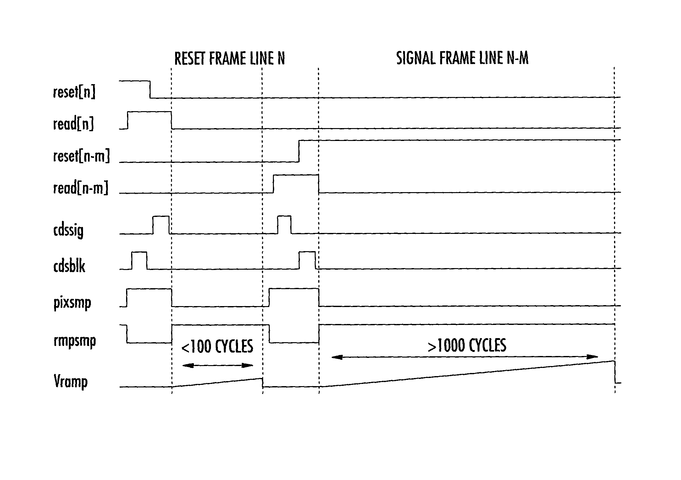
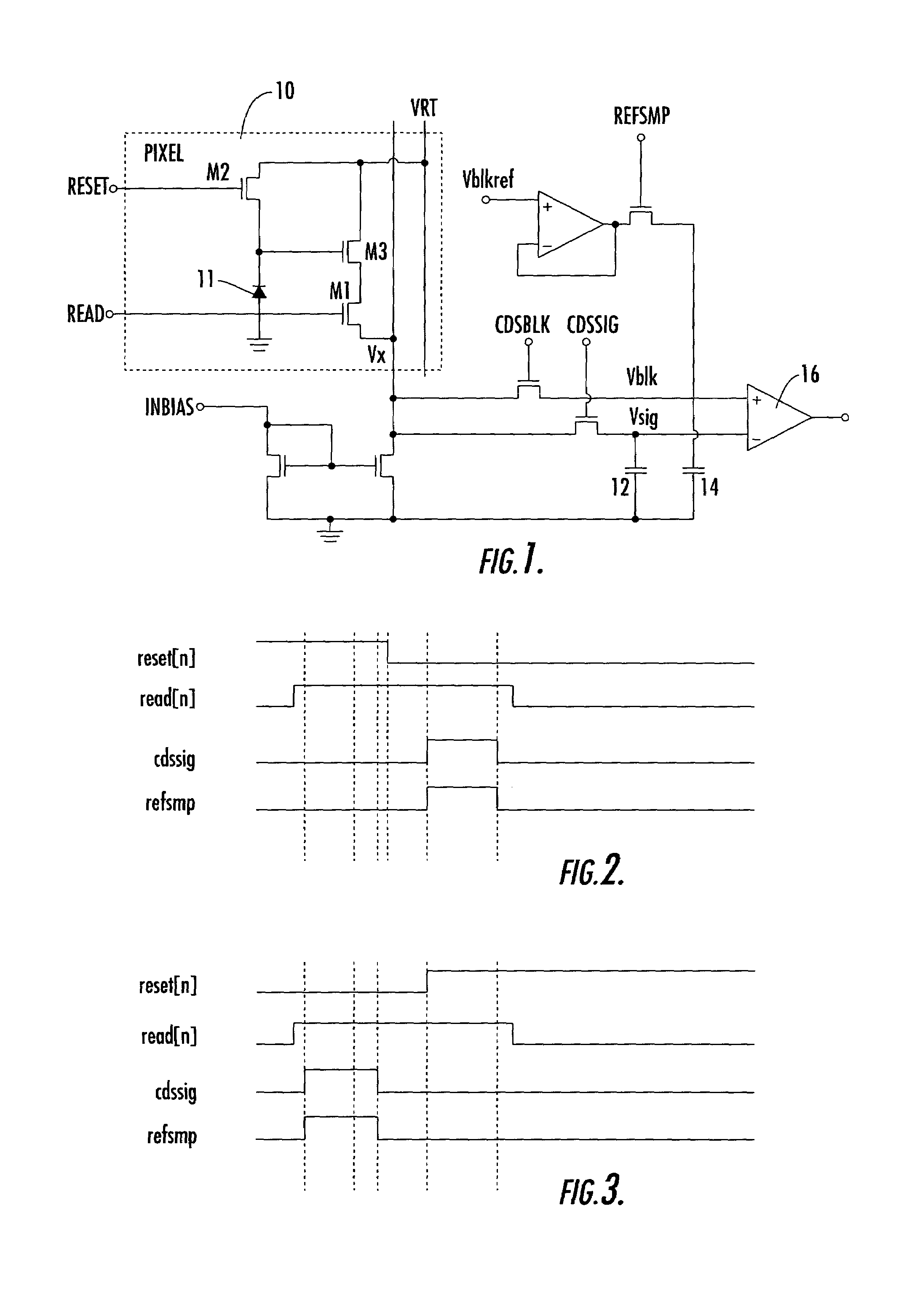
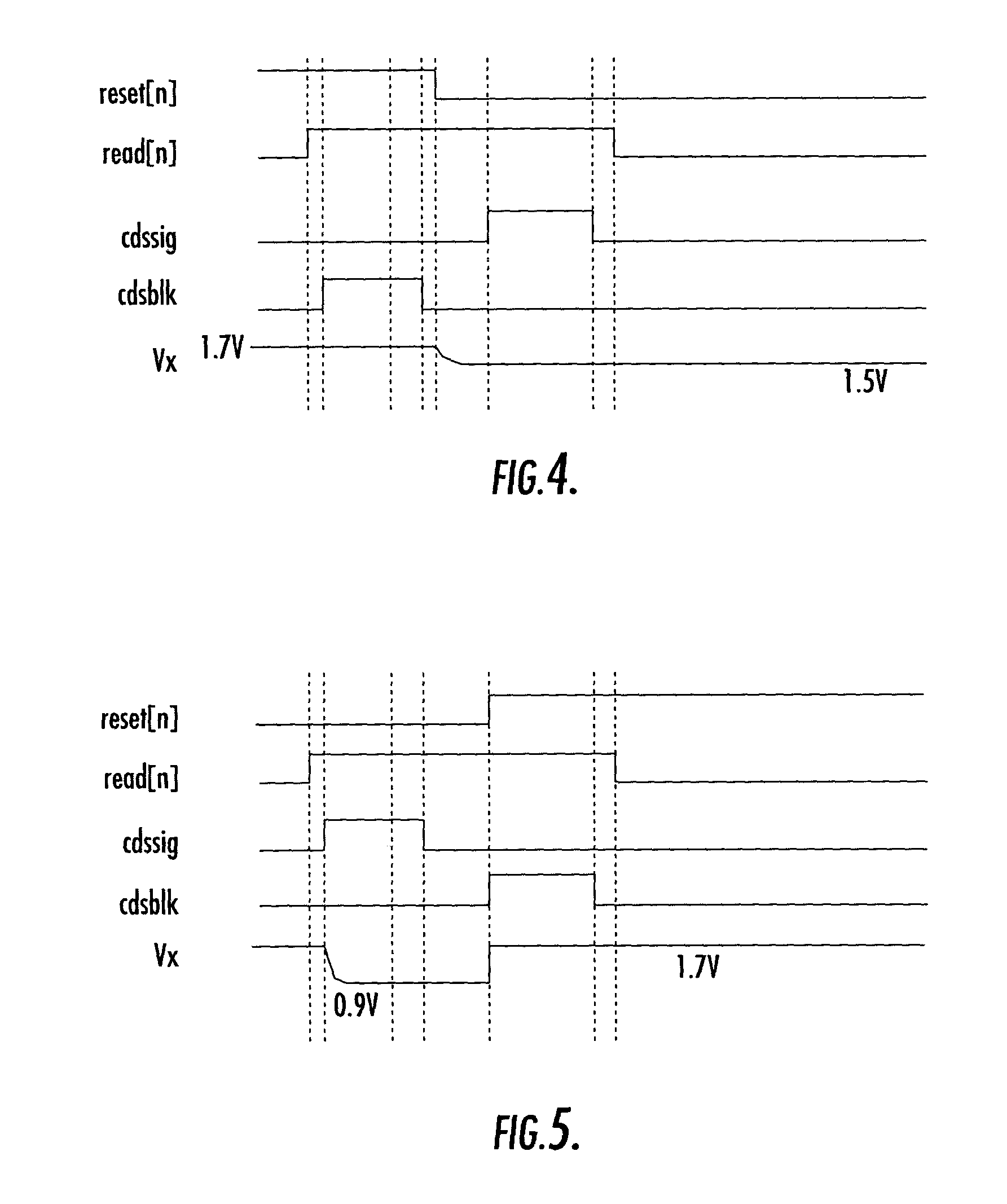
[0014]Referring to FIG. 1, an image sensor has an array of active pixels, such as 3-transistor pixels one of which is seen at 10, each pixel comprising a photodiode 11 and transistors M1, M2, M3. Each column shares a reset voltage line VRT and a read line Vx. The column has sampling capacitors 12 and 14 connected as inputs to a comparator 16. Alternatively, it is equally possible to make use of horizontal reset voltage lines.
[0015]FIG. 2 shows the timing of the known double read system. Pixel row n is released from reset by the falling edge of reset[n]. Signals REFSMP and CDSSIG then pulse simultaneously to sample the black reference voltage Vblkref as Vblk and the pixel output voltage is Vsig. The AD conversion processes the sampled differential voltage:
Vadc1=Vblkref−(VRT−Vgsn−Vrst−Vnrst)
for each column, where Vgsn is the source follower gate-source voltage and Vnrst is the kT / C noise. The samples Vadc1 are placed in a frame buffer.
[0016]After an exposure time, row n is re-read and...
PUM
 Abstract
Description
Claims
Application Information