Semiconductor memory device and a method for arranging signal lines thereof

a memory device and semiconductor technology, applied in the field of semiconductor memory devices, can solve problems such as the increase in the number of abnormal operations

Active Publication Date: 2007-10-09
SAMSUNG ELECTRONICS CO LTD
View PDF7 Cites 3 Cited by
  • Summary
  • Abstract
  • Description
  • Claims
  • Application Information

AI Technical Summary

Benefits of technology

[0015]It is an object of the present invention to provide a semiconductor memory device and a method for arranging signal lines thereof which can remove a skew occurring between data signals transmitted through global data IO signal lines due to memory cell array location in the device and that can prevent an abnormal operation which may occur during a precharge operation.

Problems solved by technology

The resulting skew can cause an abnormal operation of the semiconductor memory device if it exceeds, for example, a predetermined limit, and since the operation speed of the semiconductor device is high, the predetermined limit is smaller, thus an increase in the number of abnormal operations may occur.

Method used


Image

  • Semiconductor memory device and a method for arranging signal lines thereof
  • Semiconductor memory device and a method for arranging signal lines thereof
  • Semiconductor memory device and a method for arranging signal lines thereof

Examples


first embodiment

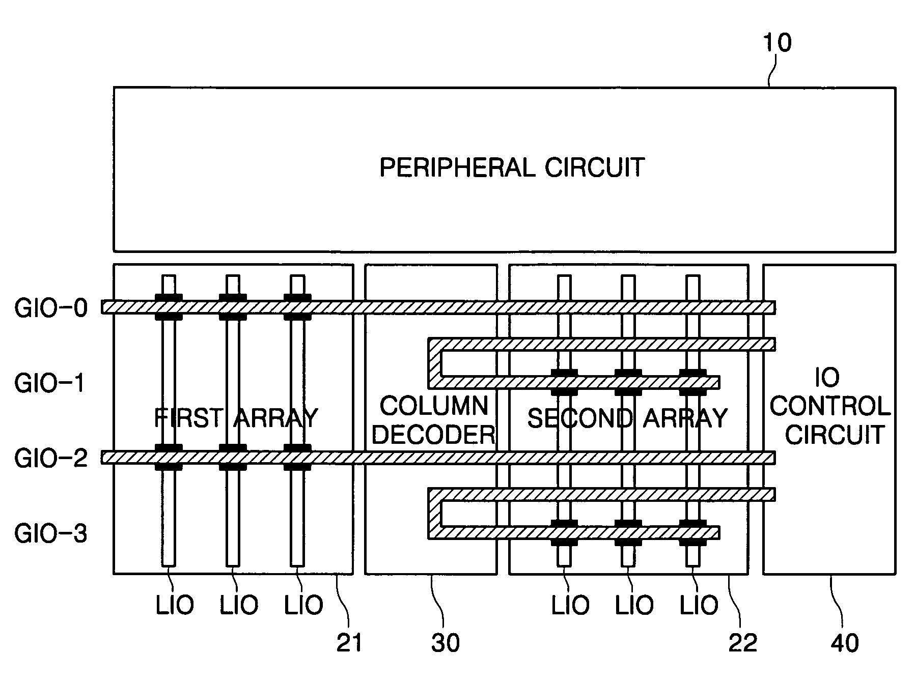
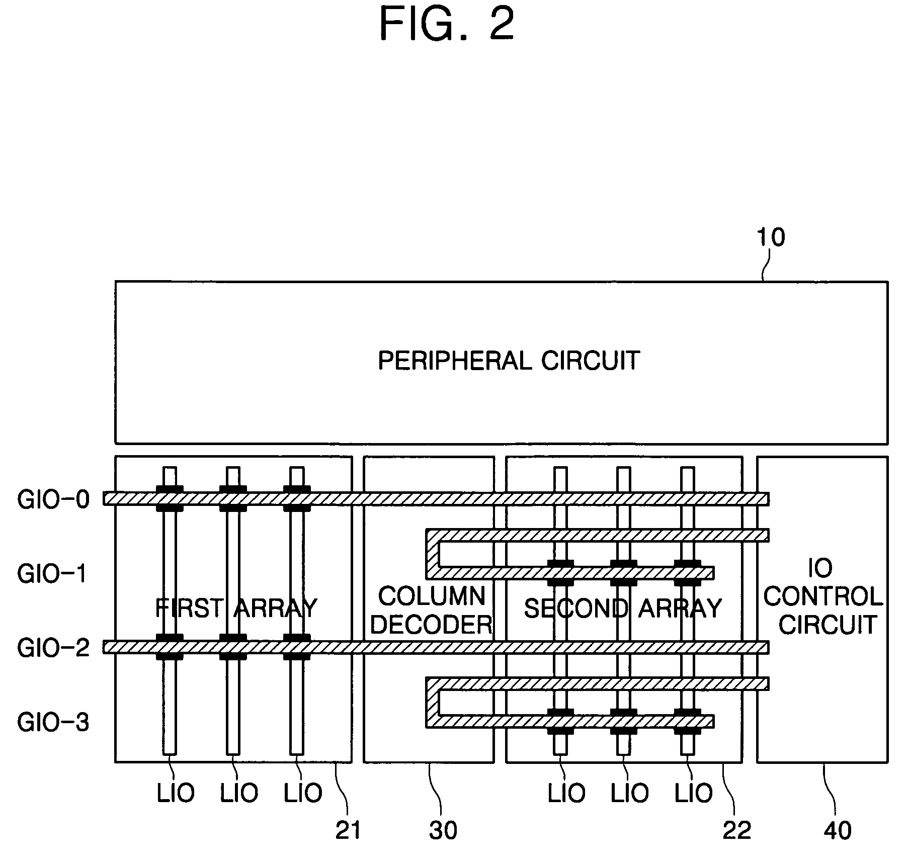
[0044]FIG. 2 is a schematic view illustrating a signal line arrangement of a semiconductor memory device according to the present invention.

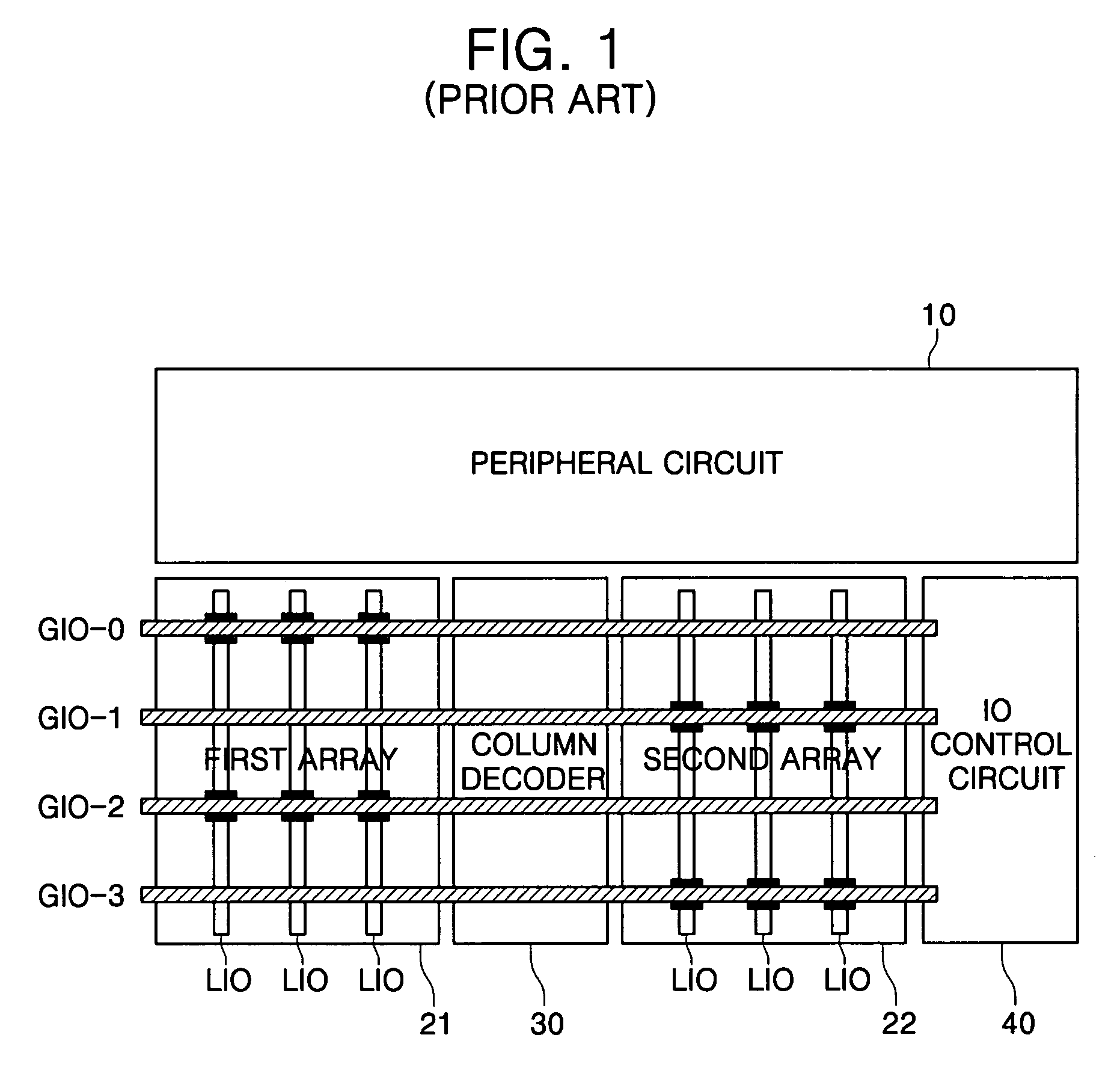
[0045]The function and arrangement of a peripheral circuit 10, first and second memory cell arrays 21 and 22, and IO control circuit 40 of FIG. 2 are the same or similar to those described above with reference to FIG. 1. In addition, the local data IO signal lines LIO of FIG. 2 are arranged in the same or similar fashion as shown in FIG. 1. As in FIG. 1, non-hatched signal lines are arranged on the first layer and hatched signal lines are arranged on the second layer. Global data IO signal lines GIO-0 and GIO-2, which are connected to the local data IO signal lines LIO above the first memory cell array 21 region, are also arranged in the same or similar way as shown in FIG. 1.

[0046]As shown in FIG. 2, global data IO signal lines GIO-1 and GIO-3, which are connected to the local data IO signal lines LIO above the second memory cell array 22 regio...

second embodiment

[0048]FIG. 3 is a schematic view illustrating a signal line arrangement of a semiconductor memory device according to the present invention. The function and arrangement of a peripheral circuit 10, first and second memory cell arrays 21 and 22, and IO control circuit 40 of FIG. 3 are the same or similar to those described above with reference to FIG. 1. In addition, the local data IO signal lines LIO of FIG. 3 are arranged in the same or similar fashion as shown in FIG. 1. As in FIG. 1, non-hatched signal lines are arranged on the first layer and hatched signal lines are arranged on the second layer.

[0049]As shown in FIG. 3, a global data IO signal line GIO-1 of global data signal lines GIO-1 to GIO-3 which are connected to the local data IO signal lines LIO above the second memory cell array 22 region extends from the IO control circuit 40, passes over the peripheral circuit 10, takes a U-like turn above the column decoder 30 region and extends to the second memory cell array 22 re...

third embodiment

[0051]FIG. 4 is a schematic view illustrating a signal line arrangement of a semiconductor memory device according to the present invention. The function and arrangement of a peripheral circuit 10, first and second memory cell arrays 21 and 22, and 10 control circuit 40 of FIG. 4 are the same or similar to those described above with reference to FIG. 1. In addition, the local data IO signal lines LIO of FIG. 4 are arranged in the same or similar fashion as shown in FIG. 1. As in FIG. 1, non-hatched signal lines are arranged on the first layer and hatched signal lines are arranged on the second layer. Signal lines filled with dots in FIG. 4 are arranged on a third layer.

[0052]As shown in FIG. 4, global data IO signal lines GIO-1 and GIO-3 which are connected to the local data IO signal lines LIO above the second memory cell array 22 region are arranged such that portions which extend from the IO control circuit 40 to the column decoder 30 region without being connected to the local d...


PUM


Abstract

The present invention discloses a semiconductor memory device and a method for arranging signal lines thereof. The semiconductor memory device including a first memory cell array, an IO control circuit and a second memory cell array arranged between the first memory cell array and the IO control circuit, includes: first IO signal lines for transmitting data between the first memory cell array and the IO control circuit, wherein the first IO signal lines are connected to first data loading locations of the first memory cell array and extend in a straight line to the IO control circuit; and second IO signal lines for transmitting data between the second memory cell array and the IO control circuit, wherein the second IO signal lines are connected to first data loading locations of the second memory cell array and extend to the IO control circuit, wherein lengths of the first IO signal lines starting from the first data loading locations of the first memory cell array to the IO control circuit are identical to lengths of the second IO signal lines starting from the first data loading locations of the second memory cell array to the IO control circuit.

Description

CROSS-REFERENCE TO RELATED APPLICATION[0001]This application claims priority to Korean Patent Application No. 2004-87524, filed Oct. 29, 2004, the disclosure of which is incorporated by reference herein in its entirety.BACKGROUND OF THE INVENTION[0002]1. Technical Field[0003]The present invention relates to a semiconductor memory device and, more particularly, to a semiconductor memory device which can remove a skew occurring between data signals transmitted through global data input / output (IO) signal lines of different lengths, and a method for arranging signal lines thereof.[0004]2. Discussion of the Related Art[0005]A conventional semiconductor memory device typically includes a memory cell array region, a column decoder region, an IO control signal region, and a peripheral circuit region. The semiconductor memory device also includes local and global data IO lines for transmitting data signals from the memory cell array region to the IO control signal region. The local data IO ...

Claims


Application Information

Patent Timeline
Patent Type & Authority Patents(United States)
IPC IPC(8): G11C5/06
CPCG11C5/063G11C7/10G11C7/02
Inventor CHO, YOUNG-CHULKIM, SUNG-HOONKIM, JOUNG-YEAL
Owner SAMSUNG ELECTRONICS CO LTD
Why Eureka
Try Eureka