Inexpensive method of fabricating a higher performance capacitance density MIMcap integrable into a copper interconnect scheme

a capacitance density and capacitor technology, applied in the field of metal-insulator-metal (mim) capacitors, can solve the problems of strong limits on the performance of the device, inability to solve, and limit the reliability of the mim capacitor, and achieve the effects of low cost impact, reliability and performance, and high yield

Active Publication Date: 2007-10-16
GLOBALFOUNDRIES U S INC
View PDF20 Cites 14 Cited by
  • Summary
  • Abstract
  • Description
  • Claims
  • Application Information

AI Technical Summary

Benefits of technology

[0010]The present invention provides a method to integrate MIM capacitors into conductive interconnect levels, with low cost impact, and high yield, reliability and performance than existing integration methods. This is accomplished in the inventive method by recessing a prior level dielectric for MIM capacitor level alignment followed by deposition and patterning of the MIM capacitor films. Specifically, and in broad terms, the method of the present invention comprises the steps of:

Problems solved by technology

Because of the high resistivity associated with TiN electrodes, the prior art schemes typically exhibit high parasitic series resistance which strongly limits the performance of the devices, especially at higher frequency.
This solution is not viable because of the severe roughness issues of an Al layer.
Roughening of the bottom plate would limit the reliability of the MIM capacitor.
As the semiconductor industry introduces thinner and more exotic films into their capacitor structures embedded in interconnect layers that have higher capacitance density, the MIM capacitor functionality and reliability are diminished because the roughness causes early breakdown of the MIM capacitor dielectric by dielectric stress and field concentration.

Method used


Image

  • Inexpensive method of fabricating a higher performance capacitance density MIMcap integrable into a copper interconnect scheme
  • Inexpensive method of fabricating a higher performance capacitance density MIMcap integrable into a copper interconnect scheme
  • Inexpensive method of fabricating a higher performance capacitance density MIMcap integrable into a copper interconnect scheme

Examples


Embodiment Construction

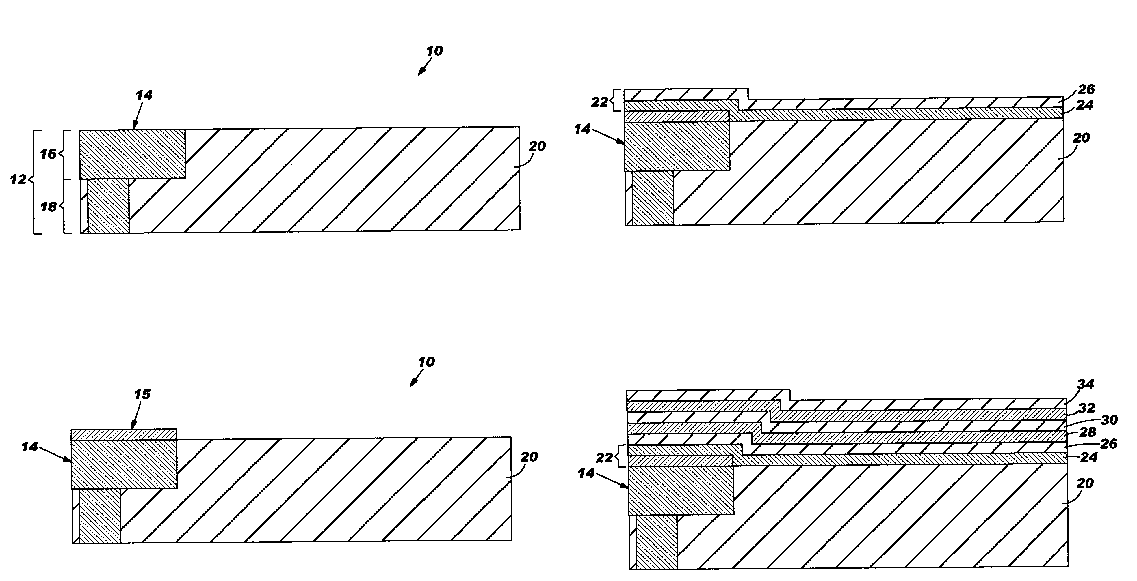
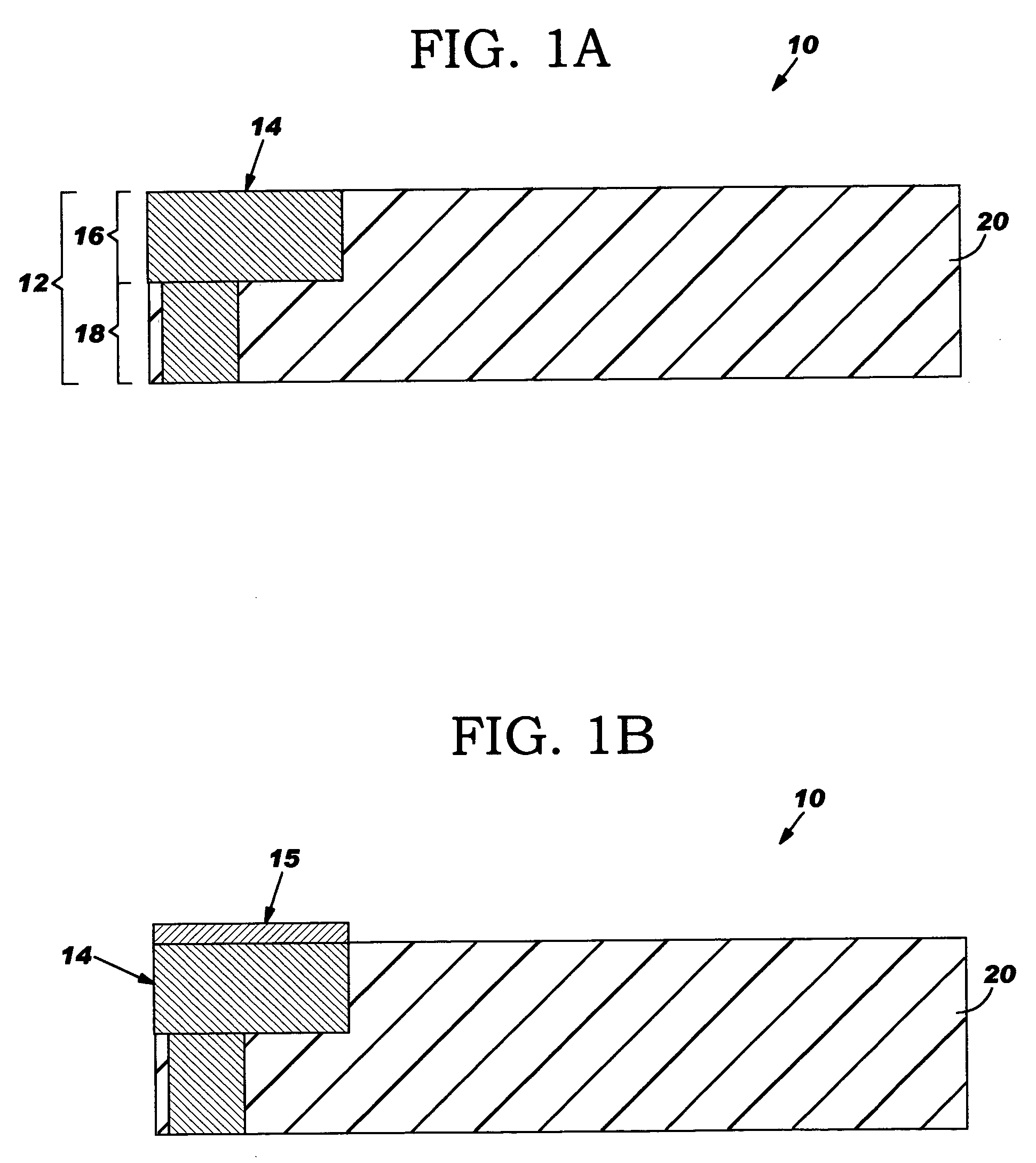
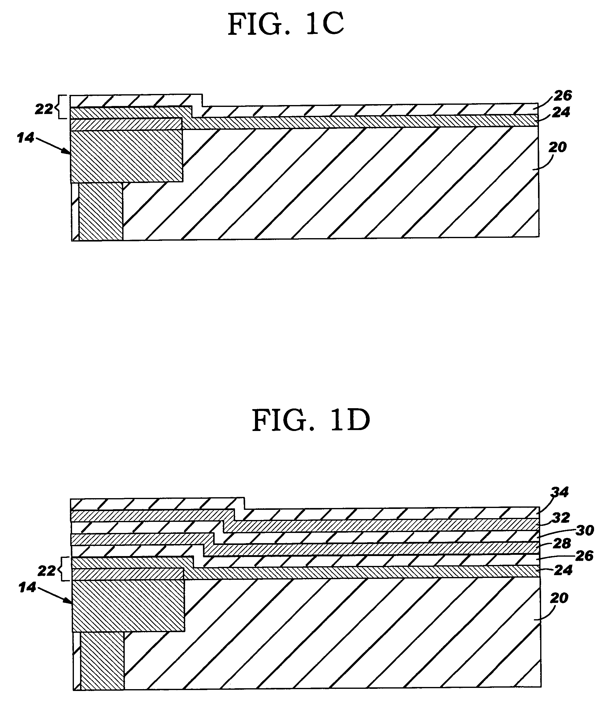
[0020]The present invention, which provides an inexpensive method of fabricating a higher performance, higher capacitance density MIM capacitor that is capable of being integrated into an interconnect scheme, will now be described in greater detail by referring to the drawings that accompany the present application. In particular, reference is made to FIGS. 1A-1G which illustrate the basic processing steps that are employed in the present invention. In the drawings that follow, the structure shown can be the first interconnect level which is formed atop a semiconductor substrate containing active devices, or alternatively, it can be any other interconnect level within an interconnect structure. It is also worth noting that although the drawings illustrate a single MIM capacitor within the structure, the present invention is not limited to that structure. Instead, a structure including multiple MIM capacitors is also contemplated herein.

[0021]Reference is first made to FIG. 1A, which...


PUM


Abstract

A method to integrate MIM capacitors into conductive interconnect levels, with low cost impact, and high yield, reliability and performance than existing integration methods is provided. This is accomplished by recessing a prior level dielectric for MIM capacitor level alignment followed by deposition and patterning of the MIM capacitor films. Specifically, the method includes providing a substrate including a wiring level, the wiring level comprising at least one conductive interconnect formed in a dielectric layer; selectively removing a portion of the dielectric layer to recess the dielectric layer below an upper surface of the at least one conductive interconnect; forming a dielectric stack upon the at least one conductive interconnect and the recessed dielectric layer; and forming a metal-insulator-metal (MIM) capacitor on the dielectric stack. The MIM capacitor includes a bottom plate electrode, a dielectric and a top plate electrode. The bottom and top plate electrodes can comprise the same or different conductive metal.

Description

BACKGROUND OF INVENTION[0001]1. Field of the Invention[0002]The present invention generally relates to semiconductor devices, and more particularly to a metal-insulator-metal (MIM) capacitor that can be used with an interconnect structure containing conductive wiring.[0003]2. Background of the Invention[0004]In the semiconductor industry, high performance capacitors are in great demand since such capacitors are essential for numerous applications, including, for example, RF and microwave. High performance capacitors have greater densities than a conventional capacitor, which leads to a reduction in chip size. Metal-insulator-metal (MIM) capacitors that are formed above back-end-of-the line (BEOL) metallurgy are also known.[0005]For example, there are several existing schemes for integrating MIM capacitors with Cu interconnects. The current working scheme employs three masks for the fabrication of the MIM capacitor and TiN films are employed as the upper and lower electrode of the MI...

Claims


Application Information

Patent Timeline
Patent Type & Authority Patents(United States)
IPC IPC(8): H01L21/8242H01L21/00H01L23/52H01L23/522
CPCH01L23/5223H01L2924/0002H01L2924/00
Inventor COOLBAUGH, DOUGLAS D.ESHUN, EBENEZER E.HE, ZHONG-XIANGMURPHY, WILLIAM J.RAMACHANDRAN, VIDHYA
Owner GLOBALFOUNDRIES U S INC
Why Eureka
Try Eureka