Image display

a multi-gradation display and image technology, applied in the field of image display, can solve the problems of difficult suppression of characteristic variations among elements, inability to allow brightness deviation in gray scale display, and difficulty in providing image display realizing multi-gradation display of six bits, so as to avoid the problem of subtle noise and increase the number of bits for multi-gradation display

Inactive Publication Date: 2007-10-23
SAMSUNG DISPLAY CO LTD +1
View PDF6 Cites 37 Cited by
  • Summary
  • Abstract
  • Description
  • Claims
  • Application Information

AI Technical Summary

Benefits of technology

[0022]An object of the present invention is therefore to provide an image display in which the number of bits for multi-gradation display is increased.
[0023]Particularly, an object of the present invention is to provide an image display realizing high-precision multi-gradation display by using both “analog signal” and “digital signal” while avoiding the problem of a subtle noise and the problem of higher drive frequency.

Problems solved by technology

By extension of the conventional technique, it is difficult to provide an image display realizing multi-gradation display of six bits, eight bits, or the like required for use in a TV or the like in future as described hereinbelow.
Particularly, in the case where a number of TFTs are formed like pixels, it is very difficult to suppress characteristic variations among elements.
Consequently, such a brightness deviation cannot be allowed in gray scale display.
Therefore, in the first conventional technique, it is difficult to realize multi-gradation gray-scale display requiring accurate brightness control.
Due to this, heavy burden is applied on a sub frame scanning circuit 212 and, as a result, it causes an increase in power consumption and cost.

Method used


Image

  • Image display
  • Image display
  • Image display

Examples


first embodiment

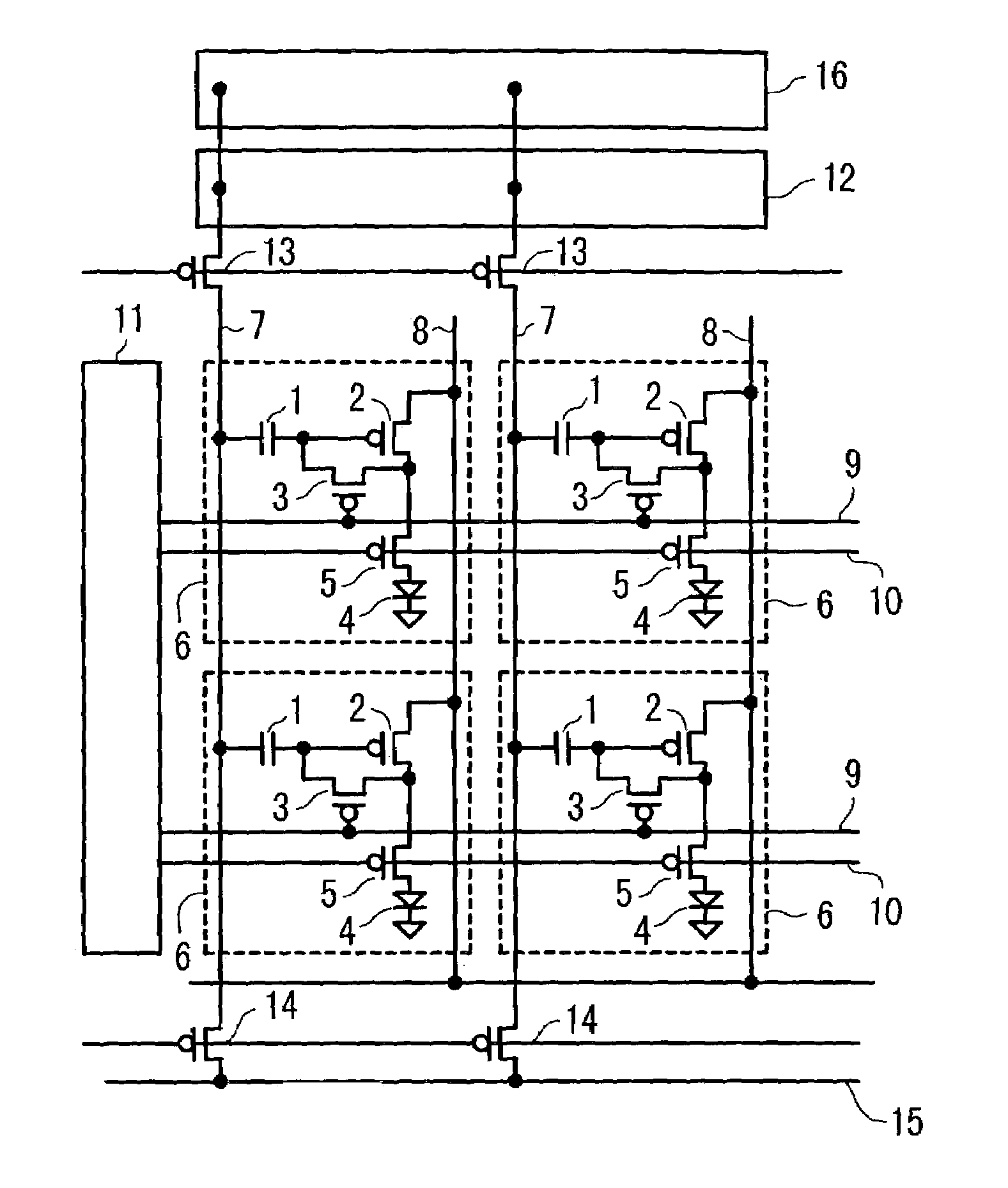
[0051]With reference to FIGS. 1 to 4, a first embodiment of an image display of the invention will be described. First, by referring to FIG. 1, the general configuration of the embodiment will be stated.

[0052]FIG. 1 is a configuration diagram of an OLED display panel of the first embodiment. Pixels 6 each having an OLED device 4 as a pixel light emitting material are arranged in a matrix in a display part. Each pixel 6 is connected to predetermined peripheral drive circuits via a writing line 9, an illuminating line 10, a signal line 7, a power source line 8, and the like. The writing line 9 and illuminating line 10 are connected to a pixel selecting circuit 11, and the signal line 7 is connected to an analog signal driving circuit 12 and a digital signal driving circuit 16 via a signal input switch 13 and is further connected to a delta wave input line 15 via a delta wave input switch 14. All of the pixels 6, pixel selecting circuit 11, analog signal driving circuit 12, and digital...

second embodiment

[0072]A second embodiment of the invention will be described by referring to FIGS. 5 and 6. FIG. 5 is a configuration diagram of an OLED display panel of the second embodiment. Pixels 25 each having an OLED device 24 as a pixel light emitting material are arranged in a matrix in a display part. Each pixel 25 is connected to peripheral drive circuits via a gate line 26, a signal line 27, a power source line 28, and the like.

[0073]In each pixel 25, the signal line 27 is connected to the gate of a drive TFT 23 and one end of a storage capacitor 22 via an input TFT 21, and one end of the drive TFT 23 and the other end of the storage capacitor 22 are commonly connected to the power source line 28. The other end of the drive TFT 23 is connected to a common power source terminal via the OLED device 24. On the other hand, one end of the gate lien 26 is connected to a gate scanning circuit 30, and one end of the signal line 27 is connected to an analog signal driving circuit 29 and a digital...

third embodiment

[0081]A third embodiment of the present invention will be described with reference to FIGS. 7 and 8. FIG. 7 is a configuration diagram of a liquid crystal display panel of the third embodiment. Pixels 34 each having a liquid crystal capacitor 33 as an optical characteristic modulation device are arranged in a matrix in a display part. The pixels 34 are connected to peripheral driving circuits via gate lines 36 and signal lines 35.

[0082]In each pixel 34, the signal line 35 is connected to one end of the liquid crystal capacitor 33 via an input TFT 32, and the other end of the liquid crystal capacitor 33 is connected to a common power source terminal. On the other hand, one end of the gate line 36 is connected to a gate scanning circuit 38, and one end of the signal line 35 is connected to an analog signal driving circuit 37 and a digital signal driving circuit 39. The input TFT 32, gate scanning circuit 38, analog signal driving circuit 37, and digital signal driving circuit 39 are f...


PUM

PropertyMeasurementUnit
parasitic capacitanceaaaaaaaaaa
currentaaaaaaaaaa
optical characteristicaaaaaaaaaa

Abstract

The present invention provides an image display capable of performing high-precision multi-gradation display while avoiding problems of a subtle noise and increase in a drive frequency. Display signal data of one frame is constructed by a plurality of sub frames of, for example, four sub frames 1/4 to 4/4. The 1/4 frame is set as an address period of an analog signal, the 2/4 frame is set as an analog gradation display period, the 3/4 frame is set as an address period of a digital signal, and the 4/4 frame is set as a digital gradation light emission period. The image display is constructed in such a manner that, in the analog gradation display period, an OLED device in a pixel emits light of time according to an analog signal voltage stored in a storage capacitor in the pixel by an analog drive signal circuit and, in the digital gradation display period, a binary light emitting operation of light emission and non light emission is performed according to a digital signal voltage stored in the storage capacitor by a digital signal driving circuit.

Description

BACKGROUND OF THE INVENTION[0001]1. Field of the Invention[0002]The present invention-relates to an image display capable of performing multi-gradation display and, more particularly, to an image display suitable for high gradation display.[0003]2. Description of the Related Art[0004]Referring to FIGS. 16 to 18, two conventional techniques will be described hereinbelow.[0005]FIG. 16 is a configuration diagram of a light emitting device using a first conventional technique (hereinbelow, called first conventional technique). Pixels 205 each having an organic electro-luminescent (EL) element 204 as a pixel light emitting material are disposed in a matrix in a display part. The pixels 205 are connected to external drive circuits via gate lines 206, source lines 207, power source lines 208, and the like. In each pixel 205, the source line 207 is connected to the gate of a power TFT 203 and one end of a storage capacitor 202 via a logic TFT (Thin-Film-Transistor) 201, and one end of the p...

Claims


Application Information

Patent Timeline
Patent Type & Authority Patents(United States)
IPC IPC(8): G09G3/32G02F1/133G09G3/20G09G3/30G09G3/36H01L51/50
CPCG09G3/2011G09G3/3648G09G3/3233G09G3/2022G09G3/2077G09G2300/0417G09G2300/0819G09G2300/0842G09G2300/0861G09G2310/0259G09G2310/027G09G2310/06G09G2320/0252G09G2320/043G09G3/2014G09G3/20
Inventor AKIMOTO, HAJIMEKINUGAWA, KIYOSHIGE
Owner SAMSUNG DISPLAY CO LTD
Why Eureka
Try Eureka