Content addressable memory (CAM) architecture and method of operating the same

a technology of addressable memory and content, applied in the field of content addressable memory (cam), can solve the problems of not being fully turned, detecting transistors, and reducing transistor sizes

Inactive Publication Date: 2007-10-23
AVAGO TECH WIRELESS IP SINGAPORE PTE
View PDF5 Cites 26 Cited by
  • Summary
  • Abstract
  • Description
  • Claims
  • Application Information

AI Technical Summary

Benefits of technology

[0027]Unlike previous designs, which typically include NMOS transistors, the present invention may include a pair of full pass gates within the compare portion of the CAM cell. For example, source-drain paths of the full pass gates may be coupled in series between a respective pair of complementary compare lines, while gate terminals of the full pass gates are coupled to the pair of storage nodes. The use of full pass gates reduces the occurrence of functional failures typically caused by voltage degrading NMOS transistors in the compare portion.
[0028]Unlike previous designs, which supply the individual bit match line signals to a common match line, the present invention uses a hierarchy of logic gates to logically combine the bit match line signals into a match line signal for the entire word (i.e., a word match line signal). In some cases, the hierarchy of logic gates may include one or more levels alternately consisting of NAND gates followed by NOR gates, depending on the number of memory cells used for storing one word and the number of inputs supplied to each gate. The hierarchical generation of a word match line enables a number of bit match lines to be combined (e.g., between 2 and 512 bit match lines) without using an excessive number of metal tracks to route the bit match lines together. For example, consider the case in which bit match line signals corresponding to a 32-bit word are combined into a word match line signal. If the 32 bit match lines were combined at the same level, a 32-input logic gate would be needed along with 32 metal tracks for routing the bit match line signals to the logic gate. The hierarchical method described herein reduces the number of metal tracks to 5 (for a 32-bit word) and enables more realistic logic gates to be used (e.g., 2 or 3-input gates).
[0031]The method described above is different from previous methods, which require the match line voltage to be restored to the previous voltage level (e.g., a preset logic H level) after a MISS occurs. By simply toggling the match line voltage between HIT and MISS states, the present invention reduces power consumption and peak current and improves the timing of the compare operation over previous designs, which continually charge, discharge and recharge the match line for every MISS that occurs. The complexity of the CAM device is also reduced, since a self-timing path is no longer needed to detect the end of a compare operation.

Problems solved by technology

The CAM cell architectures shown in FIGS. 2 and 3 present many problems, especially in newer technologies with lower power supplies and diminished transistor sizes.
This means that, in the case of a MISS, the match detect transistor (N7) will not be fully turned on.
In some cases, the degraded voltage at node C may cause functional failures, which occur when a compare operation is miss-sensed (i.e., sensed incorrectly) as either a HIT or a MISS.
The performance of memory cell 200 may further decrease over certain process, voltage and temperature (PVT) comers (especially when the temperature is low), and is often unacceptable in newer transistor technologies.
Because the transistor threshold voltage (Vth) does not drop proportionately to VDD, the threshold voltage becomes a larger percentage of VDD in newer technologies, which increases the occurrence of functional failures.
Another problem with memory cells 200 and 300 is that they tend to consume a relatively large amount of power.
Therefore, the architectures shown in FIGS. 2 and 3 consume a considerable amount of power by continually charging, discharging and recharging the match lines after each and every MISS.
In addition to increased power consumption, the need for restoring the match line to a predetermined state (after a MISS) complicates the design of the memory device and decreases the speed with which it operates.
This undesirably increases the amount of delay within a critical path.
Additional problems arise in newer technologies as gate lengths are decreased to about 0.13 μm and below.
For example, although the current leakage may be small in the 0.18 μm technology used to form memory cells 200 and 300, it becomes a bigger problem as gate lengths decrease to 0.13 μm, and often becomes unmanageable in technologies 90 nm and below.
When dynamic logic is used within the compare portion of the memory cell, as in the case of memory cells 200 and 300, more and more functional failures tend to occur as current leakage increases.
Because the match line is not actively driven during the evaluation phase (i.e., because the PMOS precharge transistor is turned off), current leakage within transistor N7 may cause the match line voltage to decrease over time.
In some cases, excessive leakage (or excessive PMOS off time) may cause the match line to be pulled down to a MISS when it should be a HIT.
Although the solution shown in FIGS. 5 and 6 may suffice in some technologies (e.g., down to about 0.13 μm the solution presents additional problems in newer technologies (e.g., 90 nm and below) where leakage constitutes a greater portion of the total transistor current consumption.
Although this may decrease the total leakage current, increasing the number of Regen cells increases the amount of area consumed by the CAM device and adds delay to the critical path.

Method used


Image

  • Content addressable memory (CAM) architecture and method of operating the same
  • Content addressable memory (CAM) architecture and method of operating the same
  • Content addressable memory (CAM) architecture and method of operating the same

Examples


Embodiment Construction

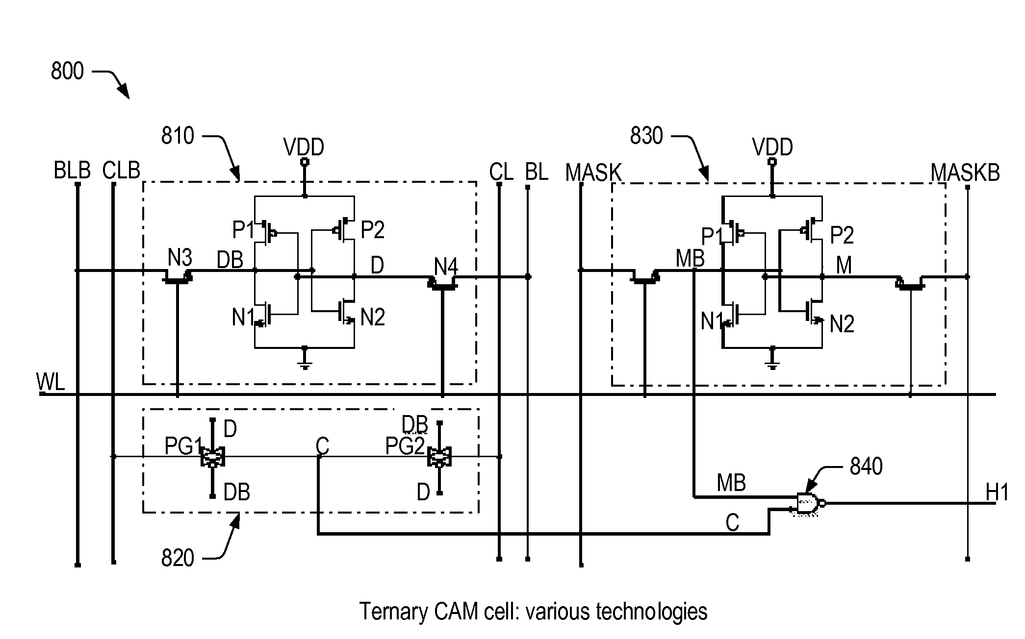
[0049]An improved CAM cell architecture and method for operating the same will now be described in reference to FIGS. 7-12. As described in more detail below, the improved architecture and method reduces power consumption and peak current, improves timing and decreases the complexity of the CAM device, as compared to conventional techniques. The improved architecture can also be implemented using a variety of technologies (including those 90 nm and below) without suffering the functional failures that typically occur in conventional designs.

[0050]FIGS. 7-8 illustrate exemplary binary and ternary CAM cell architectures, in accordance with one embodiment of the invention. As shown in FIG. 7, binary CAM cell 700 generally includes storage logic 710, comparison logic 720, a word line (WL), a match line (ML), a pair of complementary bit lines (BL / BLB) and a pair of complementary compare lines (CL / CLB). Like storage logic 210 and 310 of FIGS. 2 and 3, storage logic 710 includes a storage ...


PUM


Abstract

An improved Content Addressable Memory (CAM) architecture and method for operating the same is provided herein. The improved CAM architecture may generally include an array of memory cells arranged into rows and columns, where each row includes a number of memory cells configured for storing one word. In particular, the number of memory cells may be coupled to a plurality of local match lines which, when combined through a hierarchy of two or more logic gates, form a match line signal for the entire word. Dynamic logic is used within a compare portion of each memory cell to reduce the occurrence of functional failures. In addition, the improved method for operating the CAM reduces power consumption and peak current, and improves timing, by eliminating the need to restore the match line voltage to a preset voltage level before each new compare operation.

Description

BACKGROUND OF THE INVENTION[0001]1. Field of the Invention[0002]This invention relates to content addressable memories (CAMs) and, more particularly, to an improved CAM architecture with substantially fewer functional failures, less power consumption, and improved timing.[0003]2. Description of the Related Art[0004]The following descriptions and examples are given as background only.[0005]Content Addressable Memory (CAM) devices are typically used in applications that require the capability to quickly search for patterns stored among a group of memory cells. Just like other memory devices, a CAM is arranged as an array of memory cells, each cell being capable of storing an electric charge. These charges can be manipulated to store and recall data through the use of special control circuitry in the memory. In some cases, each memory cell may be capable of storing one of two values, depending on whether or not the cell holds a charge. The values “1” and “0” are typically used to repre...

Claims


Application Information

Patent Timeline
Patent Type & Authority Patents(United States)
IPC IPC(8): G11C15/00
CPCG11C15/04
Inventor SUN, DECHANG
Owner AVAGO TECH WIRELESS IP SINGAPORE PTE
Why Eureka
Try Eureka