Mach Zehnder photonic crystal sensors and methods
a technology of photonic crystal waveguides and sensors, applied in the field of sensors, can solve the problems of crystal oscillators, too large mass spectroscopic-based systems available today, and require too much power to be field-portabl
- Summary
- Abstract
- Description
- Claims
- Application Information
AI Technical Summary
Benefits of technology
Problems solved by technology
Method used
Image
Examples
Embodiment Construction
Definitions
[0020]Micron-scale dimensions refers to dimensions that range from 1 micrometer to a few micrometers in size.
[0021]Sub-micron scale dimensions refers to dimensions that range from 1 micrometer down to 0.05 micrometers.
[0022]Nanometer scale dimensions refers to dimensions that range from 0.1 nanometers to 50 nanometers (0.05 micrometers).
PRESENT EMBODIMENTS
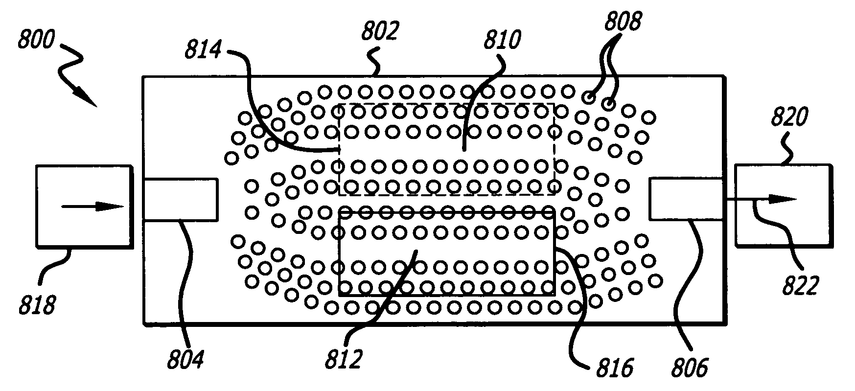
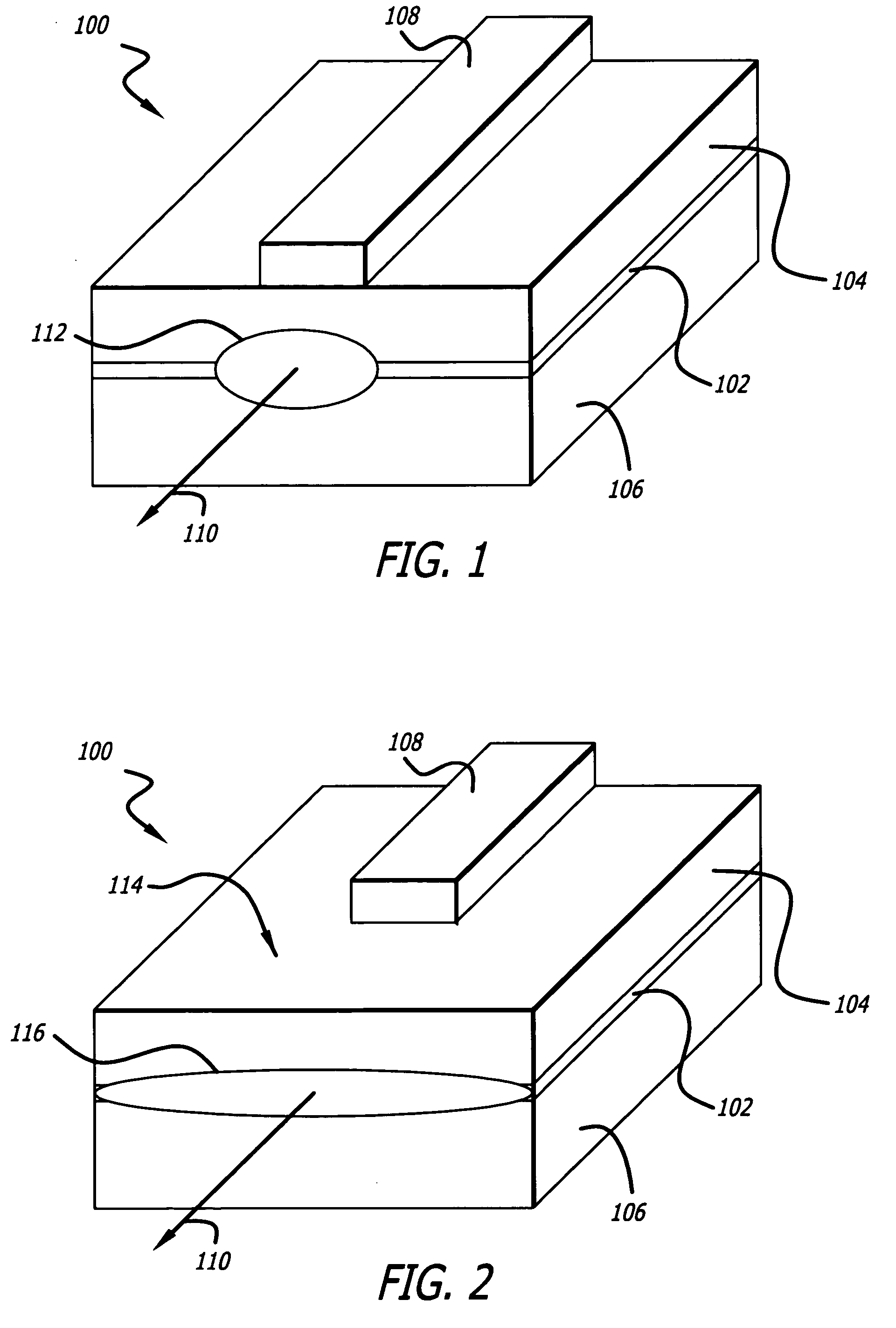
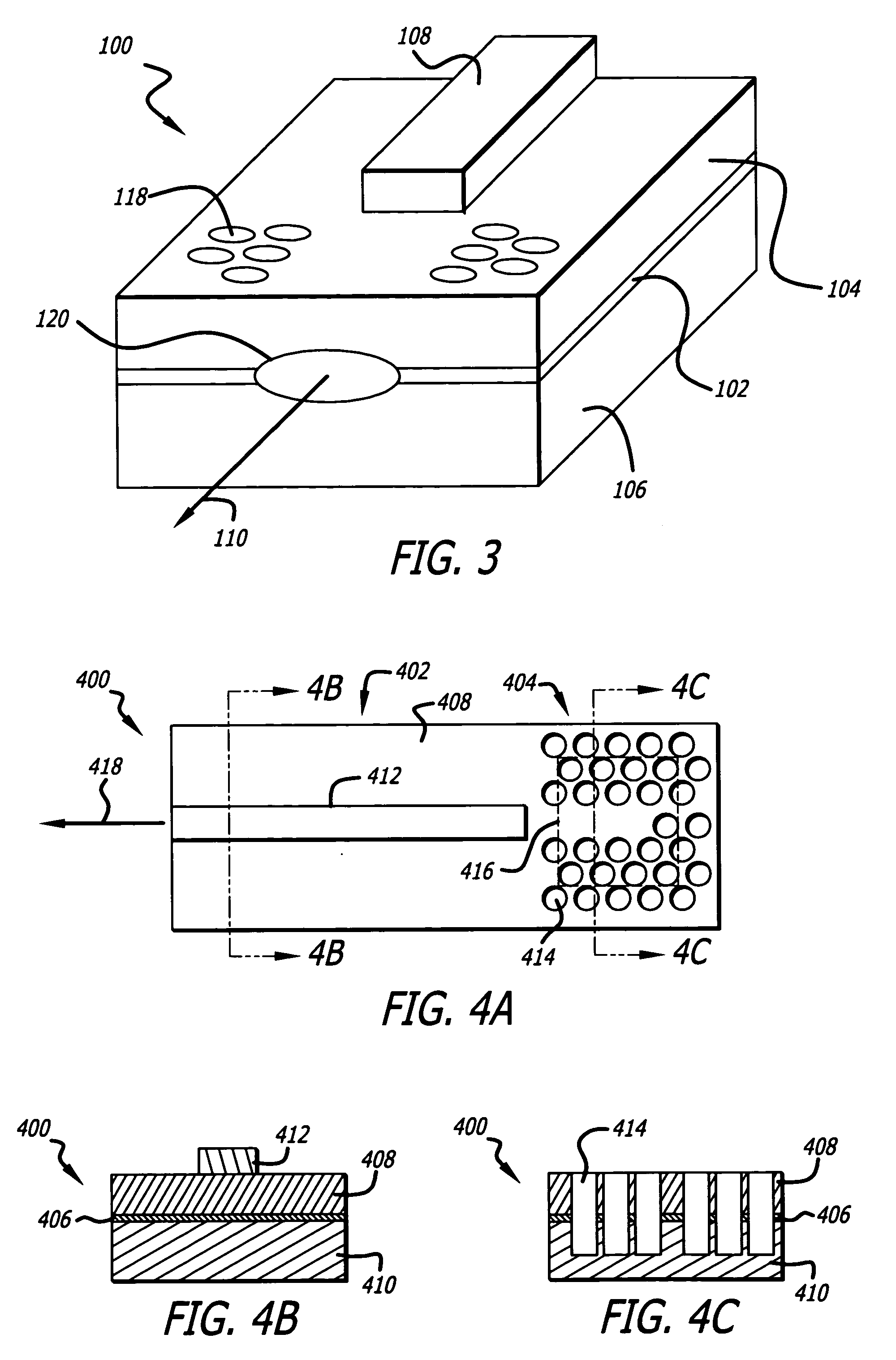
[0023]Various embodiments of the present invention pertain to interferometric and other detector structures that use photonic crystals for chemical, biological and / or other types of sensing with evanescent fields.
[0024]Evanescent fields are created by total internal reflection. FIG. 10 illustrates an example of an exponentially decaying evanescent field 1000 on the opposite side of a totally internally reflecting interface 1002 (e.g., a waveguide). When a medium of high refractive index is brought into the evanescent field, this frustrates the total internal reflection of the incident light 1004, changing the amplitude o...
PUM
 Abstract
Description
Claims
Application Information


