Photonic crystal light emitting device with multiple lattices

a light-emitting device and crystal-type technology, applied in the direction of instruments, optical elements, optics, etc., can solve the problems of poor extraction efficiency, less than 30%, and limited extraction efficiency

Active Publication Date: 2008-10-28
AGILENT TECH INC +1
View PDF48 Cites 40 Cited by
  • Summary
  • Abstract
  • Description
  • Claims
  • Application Information

AI Technical Summary

Problems solved by technology

The extraction efficiency is limited, for example, by the emitted photons suffering multiple total internal reflections at the walls of the high refractive index semiconductor medium.
As a result, the emitted photons do not escape into free space, leading to poor extraction efficiencies, typically less than 30%.
However, none of these geometries can entirely eliminate losses from total internal reflection.
A further source of loss is the reflection caused by the refractive index mismatch between the LED and the surrounding media.
However, the device of U.S. Pat. No. 5,955,749 is not operational and therefore is not a LED.
Also, electrodes are typically thought to reduce the extraction efficiency as they reflect a portion of the emitted photons back into the LED, and absorb another portion of the emitted light.
However, when electrons and holes recombine through intermediate electronic states in the electronic band gap, then the recombination energy is emitted in the form of heat instead of photons, reducing the light emission efficiency of the LED.
However, on the surface of semiconductors typically there are a large number of surface states and defect states, many of them in the electronic band gap.
This surface recombination generates heat instead of light, considerably reducing the efficiency of the LED.
However, PXLEDs include a large number of holes, thus PXLEDs have a much larger surface area than regular LEDs.
Therefore, the surface recombination may be capable of reducing the efficiency of the PXLED below the efficiency of the same LED without the photonic crystal structure, making the formation of photonic crystal structure pointless.
Since GaAs has a high surface recombination velocity, it is not a promising candidate for fabricating photonic crystal LEDs.
In particular, U.S. Pat. No. 5,955,749 does not describe the successful operation of a photonic crystal LED.
Also, U.S. Pat. No. 5,955,749 does not describe the influence of the photonic crystal on the emission process, which can affect the internal efficiency of the LED.
While photonic crystals are promising for light extraction for the reasons described above, there are problems with the design.
However, Lee et al. do not show how to form and operate a light emitting device with this design.
The addition of the electrodes, however, will substantially affect the extraction and the spontaneous emission of the LED.
Since this effect is unknown, it cannot be disregarded in the design of a LED.

Method used


Image

  • Photonic crystal light emitting device with multiple lattices
  • Photonic crystal light emitting device with multiple lattices
  • Photonic crystal light emitting device with multiple lattices

Examples


first embodiment

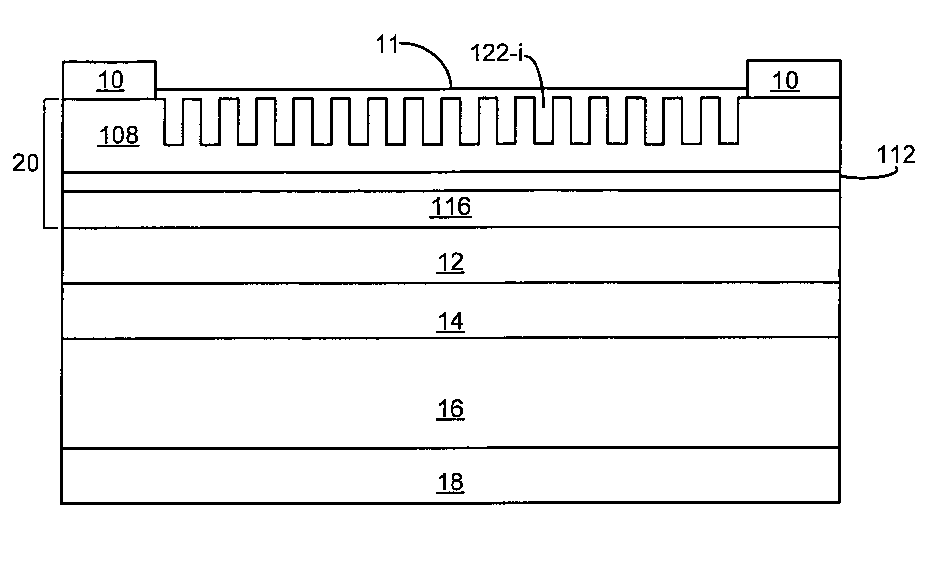
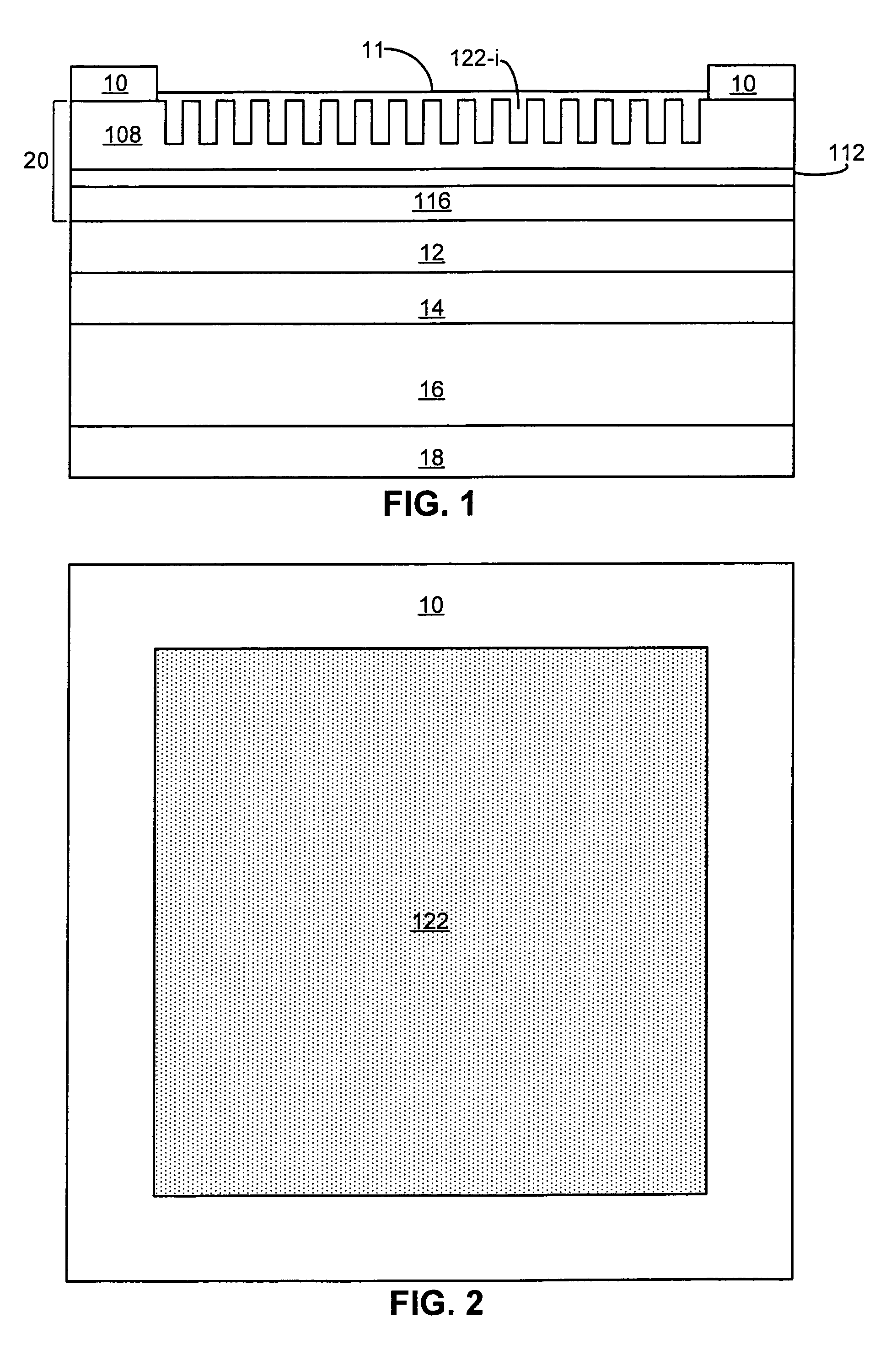
[0028]In accordance with embodiments of the invention, a photonic crystal device includes multiple lattice types. In the device, the multiple lattice types are formed on different regions of the device. At least one photonic crystal structure, referred to herein as the “enhancer photonic crystal,” is designed to optimize total radiative power (radiative efficiency), and at least one photonic crystal structure, referred to herein as the “extractor photonic crystal,” is designed to optimize light extraction (extraction efficiency).

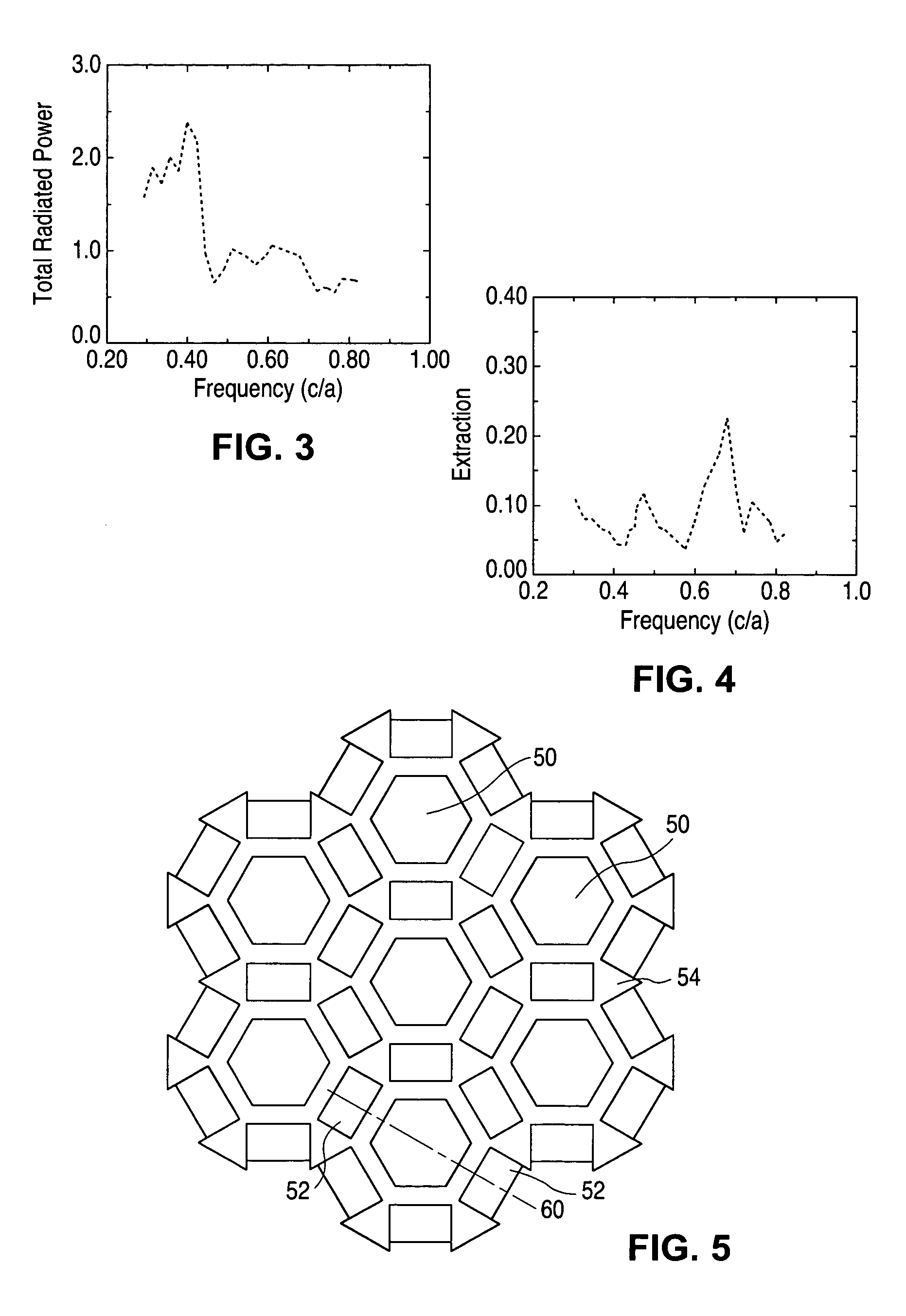
[0029]FIGS. 5 and 6 illustrate plan views of portions of devices including enhancer and extractor photonic crystals according to embodiments of the invention. In both devices, extractor photonic crystal regions 52 surround enhancer photonic crystal regions 50. A metal web 54 interposes the extractor and enhancer regions to provide current to the enhancer regions 50.

[0030]FIGS. 7 and 8 illustrate two possible cross sectional views along axis 60 of either of t...

second embodiment

[0048]In the invention, multiple lattice types are included in the same region of the device in a quasi-crystal. FIGS. 16 and 17 illustrate two examples of an arrangement of holes that form a quasi-crystal. As illustrated in FIGS. 16 and 17, a quasi-crystal is a pattern of holes located on the vertices of a repeating pattern of squares 31 and triangles 32. Such a repeating pattern is often referred to as an Archimedean lattice or a penrose tile. The lattice constant a of a quasi-crystal is the length of a side of a triangle or square in the repeating pattern. The lattice constant a and other parameters of the quasi-crystal photonic crystal, such as hole depth and diameter, may have the same ranges as described above in reference to other photonic crystal lattices. A device may incorporate a quasi-crystal as the only photonic crystal in the device, or a quasi-crystal lattice may be used as an enhancer, extractor, or reflector region as described above.


PUM


Abstract

A semiconductor light emitting device includes a photonic crystal structure that is a lattice of holes in the semiconductor layers. The photonic crystal structure includes multiple lattices. In some embodiments, the device includes a first lattice formed on a first region of the semiconductor layers and a second lattice formed on a second region of the semiconductor layers. The parameters of the first lattice may be selected to maximize the total radiated power from the device. The parameters of the second lattice may be selected to maximize the light extraction into a 30° cone on a surface of the stack.

Description

BACKGROUND[0001]1. Field of Invention[0002]The present invention relates to semiconductor light emitting devices including photonic crystal structures with multiple lattice types.[0003]2. Description of Related Art[0004]Light emitting diodes (“LEDs”) are technologically and economically advantageous solid state light sources. LEDs are capable of reliably providing light with high brightness, hence in the past decades they have come to play a critical role in numerous applications, including flat-panel displays, traffic lights, and optical communications. An LED includes a forward biased p-n junction. When driven by a current, electrons and holes are injected into the junction region, where they recombine and release their energy by emitting photons. The quality of an LED can be characterized, for example, by its extraction efficiency, which measures the intensity of the emitted light for a given number of photons generated within the LED chip. The extraction efficiency is limited, f...

Claims


Application Information

Patent Timeline
Patent Type & Authority Patents(United States)
IPC IPC(8): H01L33/00H01L33/20
CPCB82Y20/00G02B6/1225H01L33/20H01L2933/0083
Inventor WIERER, JR., JONATHAN J.SIGALAS, MIHAIL M.
Owner AGILENT TECH INC
Why Eureka
Try Eureka