Light control element and light control device

Inactive Publication Date: 2005-01-06
RICOH KK
View PDF7 Cites 39 Cited by
  • Summary
  • Abstract
  • Description
  • Claims
  • Application Information

AI Technical Summary

Benefits of technology

[0056] Thus, according to the present invention, it becomes possible to construct a light control device including an optical matrix switch formed by N×N×N optical waveguides that form a line defect in the photonic crystal structure such

Problems solved by technology

In these conventional methods, there exists an advantage of achieving large extinction ratio with simple construction, while such a conventional construction has a drawback, associated with its construction of using mechanical movement of an object such as thermal pressure generator or electromagnet, that it is difficult to achieve high-speed switching.
However, such conventional high-speed optical switches have a drawback in that the device length of several centimeters.
Because of the large device length, it is difficult to use such an optical switch for the optical interconnection switch on a circuit board carrying a semiconductor chip

Method used


Image

  • Light control element and light control device
  • Light control element and light control device
  • Light control element and light control device

Examples


first embodiment

[0076] Hereinafter, a first embodiment of the present invention will be described with reference to FIGS. 1-3.

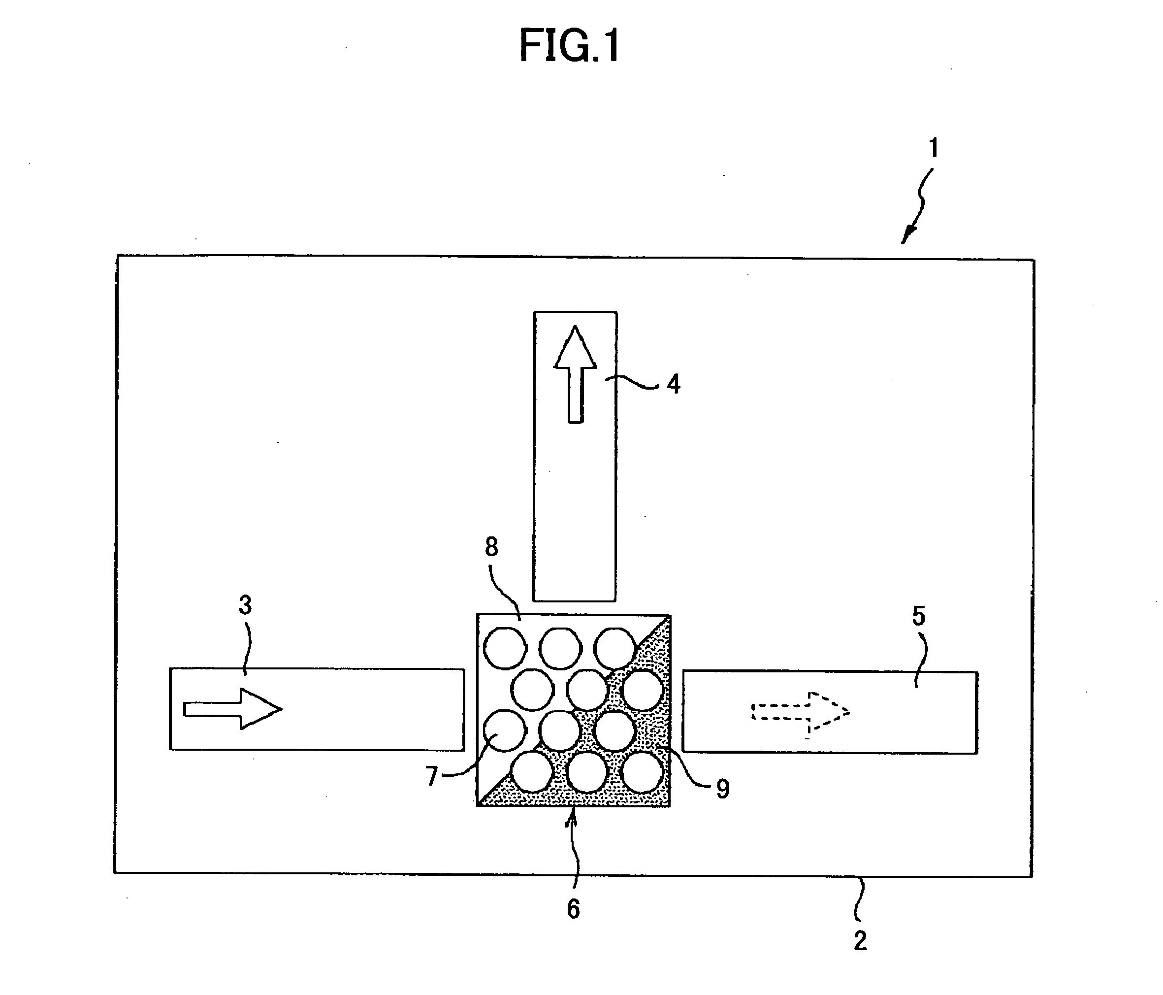
[0077]FIG. 1 a plan view shows the general construction of a light control element 1 of the present embodiment.

[0078] Referring to FIG. 1, the light control element 1 includes a substrate 2 on which three optical waveguides 3, 4 and 5 are formed, wherein the optical waveguides 3, 4 and 5 are connected with each other by an optical deflection part 6 acting as an optical coupling component. In the illustrated example, the optical waveguide 3 serves for the incident side optical waveguide, while the exit side optical waveguides 4 and 5 are provided in a perpendicular relationship with each other. It should be noted that the number of the optical waveguides is not limited to three but four or more optical waveguides may be provided. Further, the incident side optical waveguide and the exit side optical waveguide are not necessarily connected to the optical deflection part 6 an...

second embodiment

[0119] Next, a second embodiment of the present invention will be described with reference to FIG. 4 showing a plan view of a light control element 11 according to the second embodiment.

[0120] Referring to FIG. 4, the light control element 11 of the present embodiment is constructed on a substrate not illustrated and includes three optical waveguides 12, 13 and 14 formed on the substrate with an mutual angle of 120 degrees, wherein there is provided an optical deflection part 15 on the substrate at the center of the optical waveguides 12, 13 and 14 in the form of an equilateral triangle. Thereby, each end of the optical waveguides 12, 13 and 14 is connected to the optical deflection part15.

[0121] It should be noted that the ends of the optical waveguides 12, 13 and 14 connected to the optical deflection part 15 carry thereon photonic crystals 16, 17 and 18 respectively, wherein the photonic crystals 16, 17 and 18 constitute a variable refractive index part that can control the tra...

third embodiment

[0125]FIG. 5 shows the construction of a light control element 21 according to a third embodiment of the present invention in a plan view.

[0126] Referring to FIG. 5, the light control element 21 of the present embodiment is constructed on a substrate not illustrated and includes four optical waveguides 22-25 formed on the substrate in a cross pattern crossing with each other perpendicularly. At the center of the optical waveguides 22-25, there is provided an optical deflection part 26 having a square form as an optical coupling component, and each of the optical waveguides 22-25 has its end connected to such an optical deflection part 26. Here, it should be noted that the number of the optical waveguide is not limited to four but five or more optical waveguides may be provided. On the other hand, when the number of the optical waveguides is increased, there is caused correspondence increase of the connection part similarly to the case of the second embodiment, and there is a possib...


PUM


Abstract

A light control element includes a substrate, an optical coupling component formed on the substrate by a photonic crystal structure, and a variable refractive index part provided in a part of the photonic crystal structure so as to divide The optical coupling component into two regions, wherein a traveling direction of a light is changed at an interface of the regions by changing a refractive index at the variable refractive index part such that there is caused a reflection for at least one wavenumber of the light.

Description

BACKGROUND OF THE INVENTION [0001] The present invention is related to light control elements and light control devices using a photonic crystal structure and applicable to light switches, optical intensity modulators, and the like. [0002] A photonic crystal forms a photonic bandgap, which is a forbidden band of photons, as a result of dielectric periodical structure having a period corresponding to optical wavelength and exhibits singular effects due to its strong dispersion. Thus, photonic crystals are expected as an ultra minute optical integrated circuits or novel functional optical devices. By using these properties, it becomes possible to construct light control elements such as light switches or optical intensity modulators having an extremely minute optical path modification function. [0003] Various structures are proposed for optical path switching devices according to the applications and according to the materials used therefor. For example, Japanese Laid-Open Patent Appl...

Claims


Application Information

Patent Timeline
IPC IPC(8): G02B6/122G02B6/125
CPCB82Y20/00G02B6/125G02B6/1225
Inventor SAKAI, ATSUSHIKATOH, IKUO
Owner RICOH KK
Why Eureka
Try Eureka