MEMS device integrated chip package, and method of making same

a technology of integrated circuit chips and semiconductor devices, applied in the direction of microstructural devices, capacitors with electrode distance variation, transportation and packaging, etc., can solve the problems of structure that is not compatible with integrated fabrication schemes, and uneconomical real estate cost to place semiconductor device silicon. to achieve the effect of facilitating the removal of temporary filler materials

Inactive Publication Date: 2007-11-06
INTEL CORP
View PDF8 Cites 24 Cited by
  • Summary
  • Abstract
  • Description
  • Claims
  • Application Information

AI Technical Summary

Benefits of technology

[0035]FIG. 25 illustrates further alternative processing of the resonator beam structure taken along the sect...

Problems solved by technology

One of the difficulties of integrated circuit packaging is that selected large, usually passive devices that may be placed on silicon with an IC, have structures that are not compatible with the integrated fabrication scheme of the traditional active components such as field effect devices and metallization wiring layouts.
For example, on an active surface of a device that requires quality factor inductors, it becomes difficult integrate into the fabrication scheme a large-enough conductive structure to have the high inductance (Q) that may be required.
Similarly, where a large surface area is needed for a specific capacitor, the real estate cost to place it on the semiconductor device silicon is uneconomical.
Another problem relates to prior art on-ch...

Method used


Image

  • MEMS device integrated chip package, and method of making same
  • MEMS device integrated chip package, and method of making same
  • MEMS device integrated chip package, and method of making same

Examples


Embodiment Construction

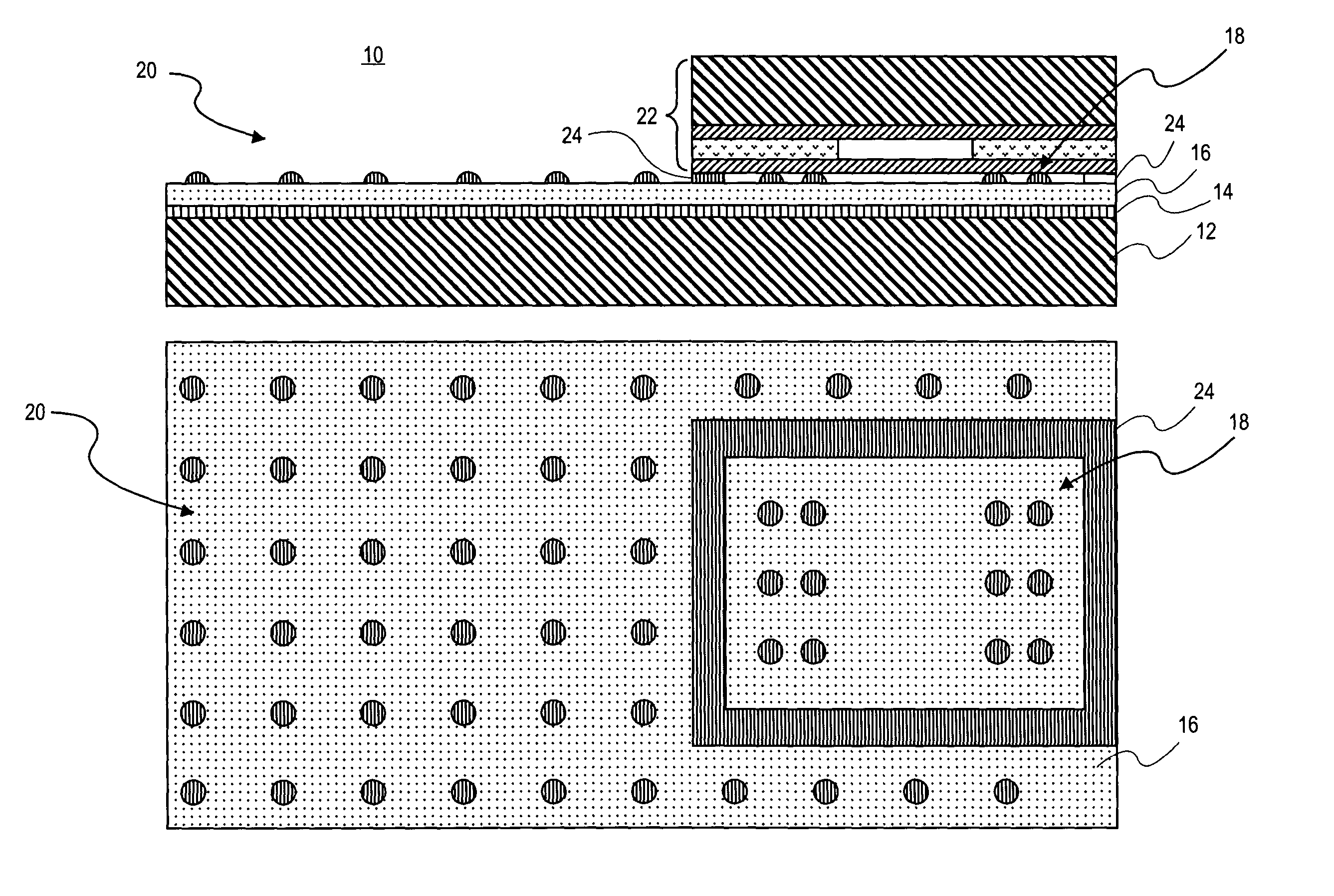
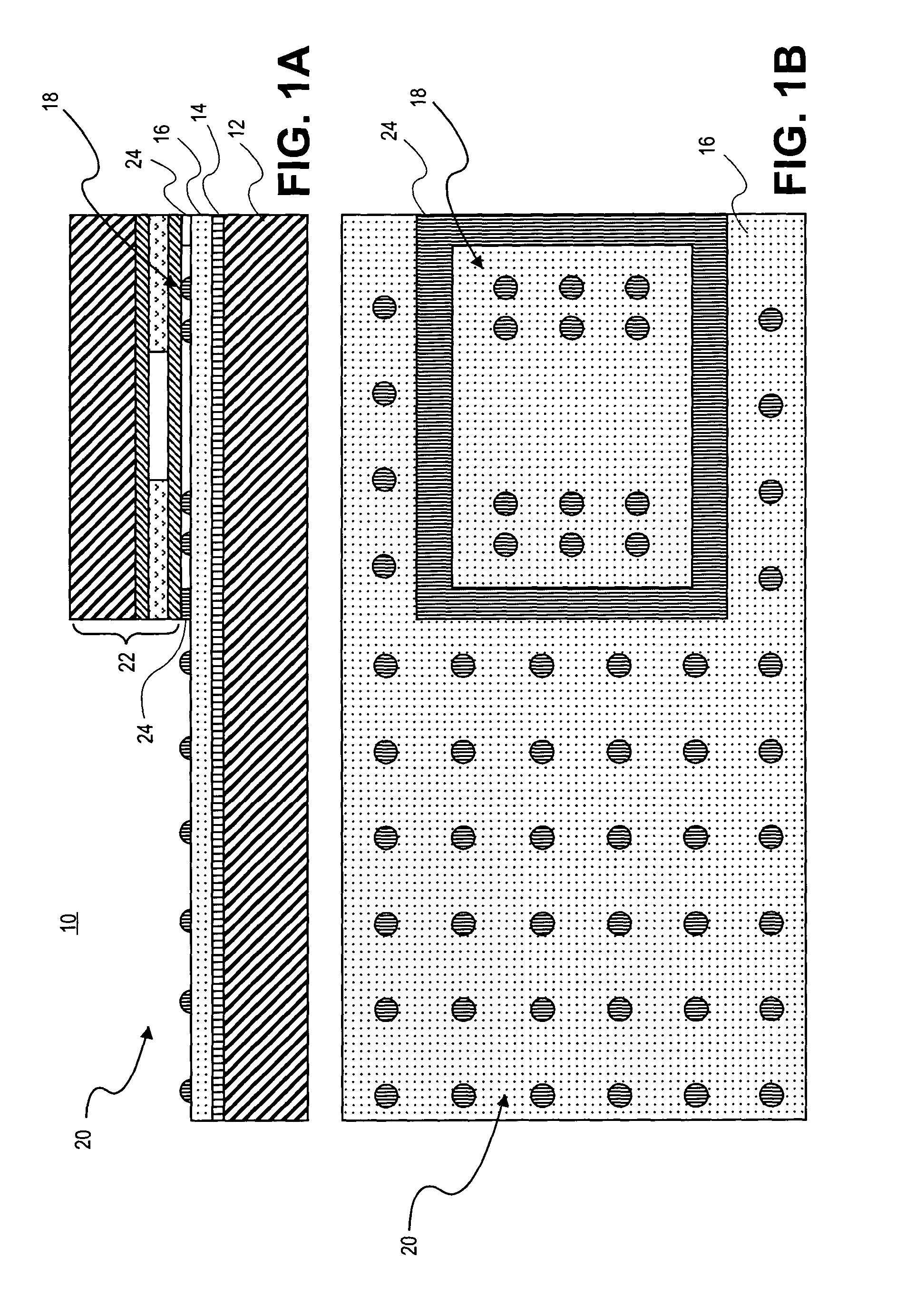
[0042]The present invention relates to a chip package that places micro electromechanical structure (MEMS) devices in a structure that is separate from the integrated circuit (IC) chip. The chip package may include a semiconductor device in one piece of silicon, and at least one MEMS in a separate structure such as a separate piece of silicon or like, or a printed circuit board or the like. The semiconductor device and the at least one MEMS comprise an integrated package.

[0043]FIG. 1a is an elevational side view of a MEMS package 10 during fabrication. MEMS package 10 includes a semiconductor device 12 with an active surface 14 and dielectric layer 16 such as an interlayer dielectric layer (ILD). Upon dielectric layer 16 is disposed a first electrical contact array 18 over active surface 14 and a second electrical contact array 20 also over active surface 14. Above active surface 14 is disposed a first MEMS 22. First MEMS 22 may be by way of non-limiting example, selected from a cap...


PUM


Abstract

The present invention relates to a chip package that includes a semiconductor device and at least one micro electromechanical structure (MEMS) such that the semiconductor device and the MEMS form an integrated package. One embodiment of the present invention includes a semiconductor device, a first MEMS device disposed in a conveyance such as a film, and a second MEMS device disposed upon the semiconductor device through a via in the conveyance.
The present invention also relates to a process of forming a chip package that includes providing a conveyance such as a tape automated bonding (TAB) structure, that may hold at least one MEMS device. The method is further carried out by disposing the conveyance over the active surface of the device in a manner that causes the at least one MEMS to communicate electrically to the active surface. Where appropriate, a sealing structure such as a solder ring may be used to protect the MEMS.

Description

CROSS-REFERENCE TO RELATED APPLICATIONS[0001]This application is a divisional of U.S. patent application Ser. No. 09 / 687,907, filed Oct. 12, 2000, and claims priority therefrom under 35 U.S.C.§ 120. The priority application has issued as U.S. Pat. No. 6,621,137.BACKGROUND OF THE INVENTION[0002]1. Field of the Invention[0003]The present invention relates generally to integrated circuit chip (IC) packaging. More particularly, the present invention relates to the packaging devices with an integrated circuit chip package. In particular, the present invention relates to integrated packaging of a microelectronic device with devices such as switches, capacitors, filters, resonators, inductors, and power supplies.[0004]2. Description of Related Art[0005]One of the difficulties of integrated circuit packaging is that selected large, usually passive devices that may be placed on silicon with an IC, have structures that are not compatible with the integrated fabrication scheme of the tradition...

Claims


Application Information

Patent Timeline
IPC IPC(8): H01L21/461H01L21/311H01L27/108H01L29/00
CPCB81C1/00333H01G5/40H01G5/16Y10T428/24248H01L2224/48091H01L2924/00014
Inventor MA, QINGCHENG, PENGRAO, VALLURI
Owner INTEL CORP
Why Eureka
Try Eureka