High-speed solid-state imaging device capable of suppressing image noise
a solid-state imaging and high-speed technology, applied in the field of solid-state imaging devices, can solve the problems of image noise, such as vertical lines, image noise, image noise, etc., and achieve the effects of reducing parasitic capacitance, reducing noise, and speeding up circuit operation
- Summary
- Abstract
- Description
- Claims
- Application Information
AI Technical Summary
Benefits of technology
Problems solved by technology
Method used
Image

Examples
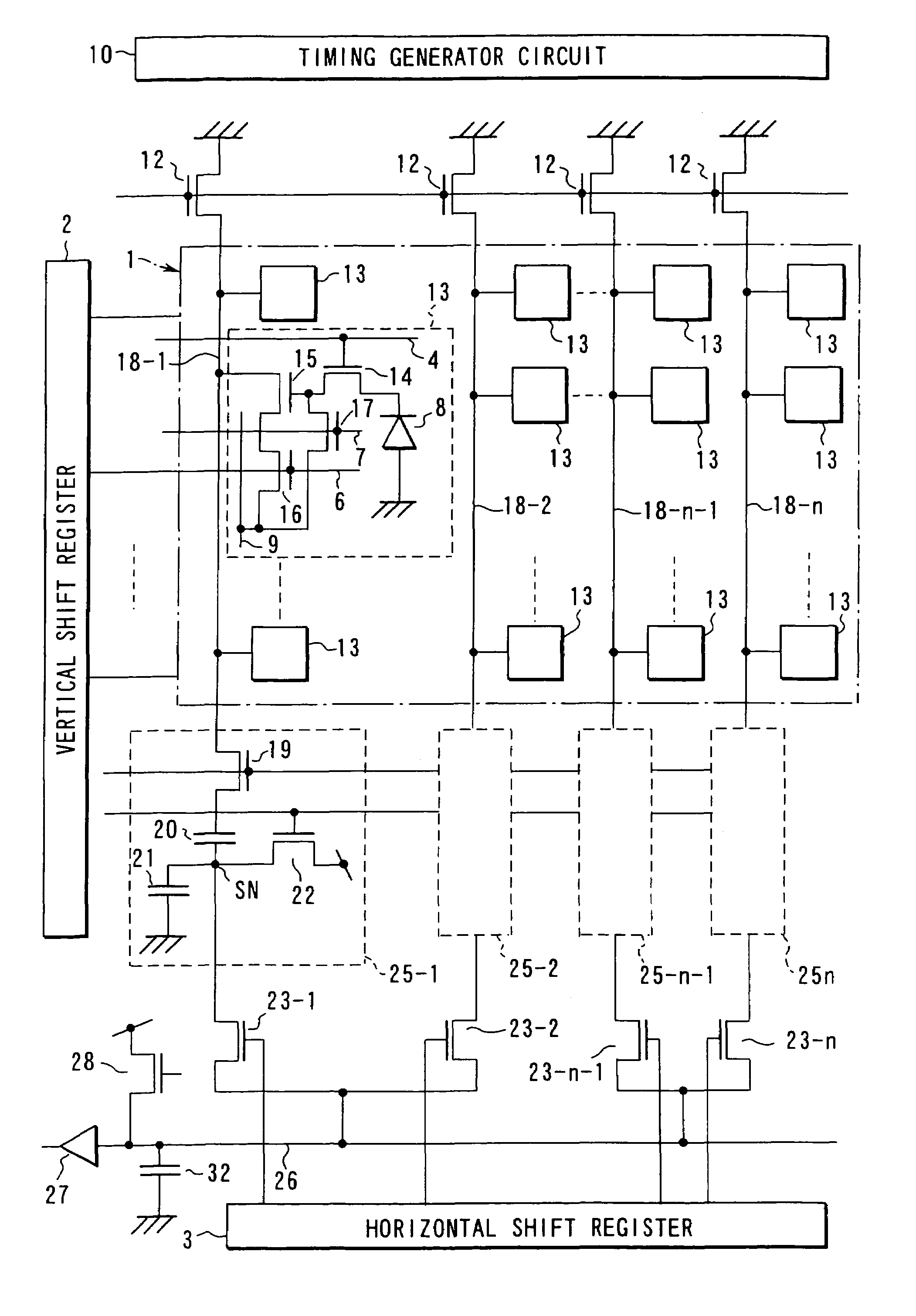
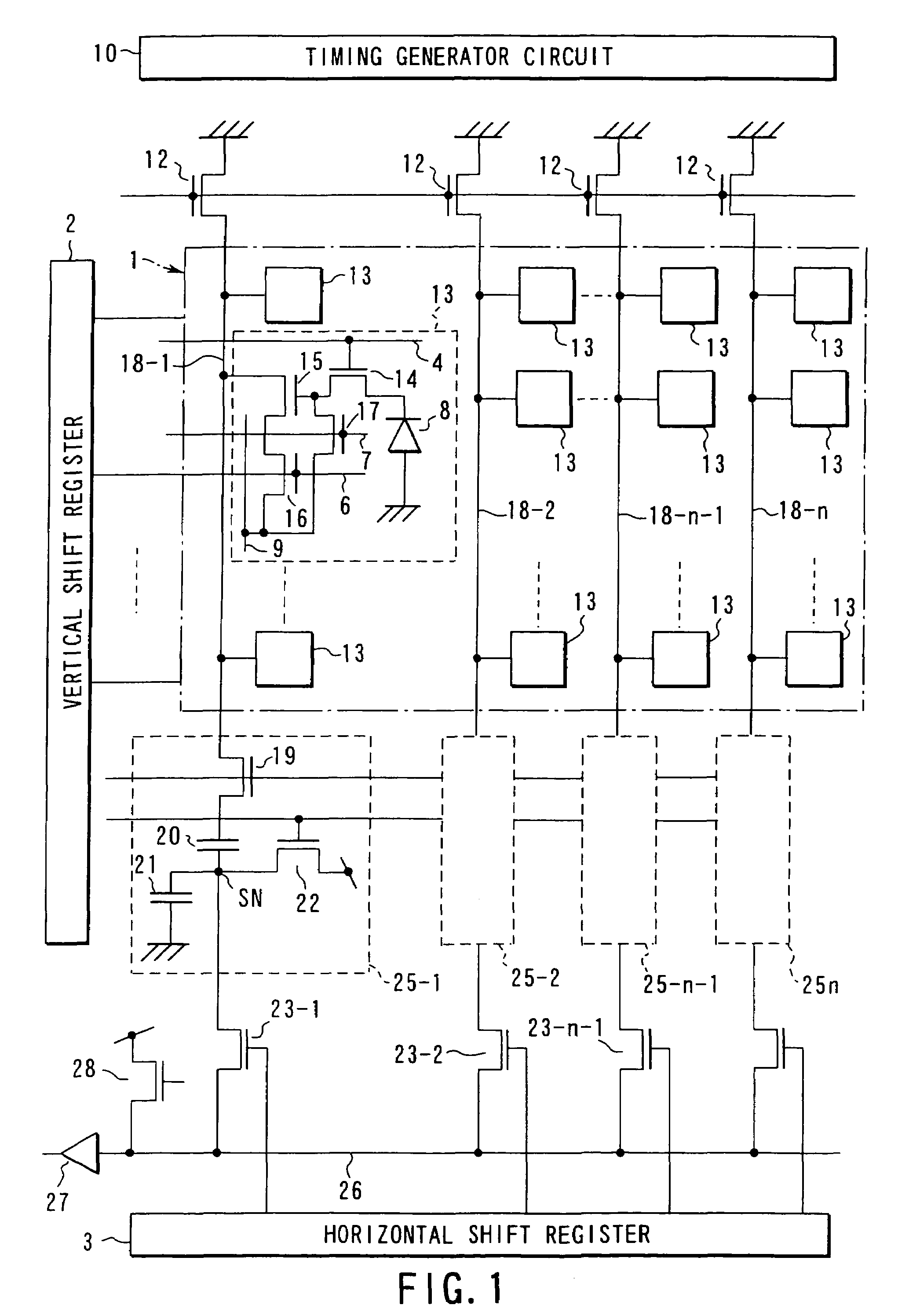
first embodiment
Modification 2 of First Embodiment
[0103]A COMO image sensor according to modification 2 of the first embodiment is the same as the CMOS image sensor of the first embodiment, except that at least the clamp potential of the potential clamping transistor 22 connected to the signal storage node SN of the noise chancellor circuit 25-i and the reset potential of the horizontal reset transistor 28 connected to the horizontal signal line 26 are set to, for example, about 1V in a period during which horizontal select transistors 23-i select and read sequentially the signals stored at the signal storage nodes SN of the individual noise chancellor circuits 25-i.
[0104]With such a configuration, after the noise removing operations have been completed, one end of the clamping potential side of the potential clamping transistor 22 is biased in the reverse direction with respect to the substrate region (in the embodiment, p-well=0V), which suppresses the leakage current. This suppresses a voltage d...
second embodiment
[0109]FIG. 3 shows an equivalent circuit of a CMOS image sensor according to a second embodiment of the present invention.
[0110]The image sensor of FIG. 3 is the same as the CMOS image sensor of conventional equivalent 1 in FIG. 20, except that bias applying transistors 31 and an on / off control circuit 32 are added. The bias applying transistors 31 are connected between the respective vertical signal lines 18-i and bias voltage nodes to set at a desired bias potential (e.g., about 1V) the voltages on the vertical signal lines 18-i after a series of noise removing operations by the noise chancellor circuits 25-i has been completed in a read operation for each horizontal line. The on / off control circuit 32 not only turns off the load transistors 12 of the vertical signal lines 18-i, but also turns on the bias applying transistors 31 after a series of noise removing operations has been completed. In FIG. 3, the same parts as those of FIG. 20 are indicated by the same reference symbols ...
third embodiment
[0115]FIG. 5 shows an equivalent circuit of a CMOS image sensor according to a third embodiment of the present invention.
[0116]The image sensor of FIG. 5 is the same as the CMOS image sensor of conventional equivalent 2 of FIG. 22, except that there is provided a load transistor on / off control circuit 50 (source follower control switch circuit) which not only turns off the load transistor TL of the vertical signal line VLIN but also brings the vertical signal line VLIN to a specific bias voltage (e.g., power supply voltage VDD=about 3.3V) after a series of noise removing operation has been completed, and that the configuration of the pulse selector (driving circuit) 2a, that of the timing generator circuit 10, and that of the bias generator circuit 11a differ from those of conventional equivalent 2.
[0117]Specifically, in FIG. 5, unit cells 13 are arranged in the cell area (imaging area) 1 in a two-dimensional matrix. Each unit cell 13 is composed of a vertical select transistor (row...
PUM
 Abstract
Description
Claims
Application Information