Multilayer electronic component and manufacturing method thereof

a technology of electronic components and manufacturing methods, applied in the direction of foil-based vessel movement reduction, fixed capacitor details, vessel construction, etc., can solve the problems of complicated manufacturing steps, displacement, expansion/contraction or the like of a print pattern, and cracks or delamination

Inactive Publication Date: 2007-11-13
TDK CORPARATION
View PDF11 Cites 17 Cited by
  • Summary
  • Abstract
  • Description
  • Claims
  • Application Information

AI Technical Summary

Benefits of technology

[0011]It is an object of the present invention to provide a multilayer electronic component and a manufacturing method thereof which can readily prevent a step absorption layer from getting onto an upper surface of an internal electrode or prevent a gap from being generated between the step absorption layer and the internal electrode.<Multilayer Electronic Component>
[0015]In the present invention, a side portion of at least one internal electrode layer forms an inclined surface. Moreover, at least one step absorption layer is superimposed to partially overlap the inclined surface. According to this configuration, even if pattern misalignment such as displacement or expansion / contraction is generated in a print pattern of the step absorption layer, a margin quantity for the pattern misalignment is assured. Therefore, it is possible to readily prevent the step absorption layer from getting onto the upper surface of the internal electrode layer or a gap from being generated between the step absorption layer and the internal electrode layer.
[0016]In a preferred aspect, an overlap dimension of the step absorption layer with respect to the inclined surface is less than 60 μm as seen in a plan view. According to this overlap dimension, delamination can be avoided.<Manufacturing Method of Multilayer Electronic Component>
[0020]As described above, according to the manufacturing method of a multilayer electronic component of the present invention, the internal electrode layer is formed on the dielectric green sheet in such a manner that the side portion thereof forms the inclined surface. Furthermore, the step absorption layer is superimposed and formed on the dielectric green sheet in such a manner that the end portion thereof partially overlaps the inclined surface. According to this configuration, even if pattern misalignment such as displacement or expansion / contraction is generated in a print pattern of the step absorption layer, a margin quantity for the pattern alignment is assured. Therefore, it is possible to readily prevent the step absorption layer from getting onto the upper surface of the internal electrode layer or a gap from being generated between the step absorption layer and the internal electrode layer.
[0023]As described above, according to the present invention, there can be provided the multilayer electronic component and the manufacturing method thereof which can readily prevent the step absorption layer from getting onto the upper surface of the internal electrode or a gap from being generated between the step absorption layer and the internal electrode.

Problems solved by technology

Such a step induces a crack or delamination at the time of baking, which can be a factor of deteriorating characteristics of a product or reducing a process yield.
However, at a ceramic paste print step, there actually occurs displacement, expansion / contraction or the like of a print pattern.
However, the technology described in Patent Reference 2 requires control or management of a print shift quantity, thus resulting in complicated manufacturing steps.
When the step absorption layer gets onto the upper surface of the internal electrode, a problem of delamination occurs.

Method used


Image

  • Multilayer electronic component and manufacturing method thereof
  • Multilayer electronic component and manufacturing method thereof
  • Multilayer electronic component and manufacturing method thereof

Examples


Embodiment Construction

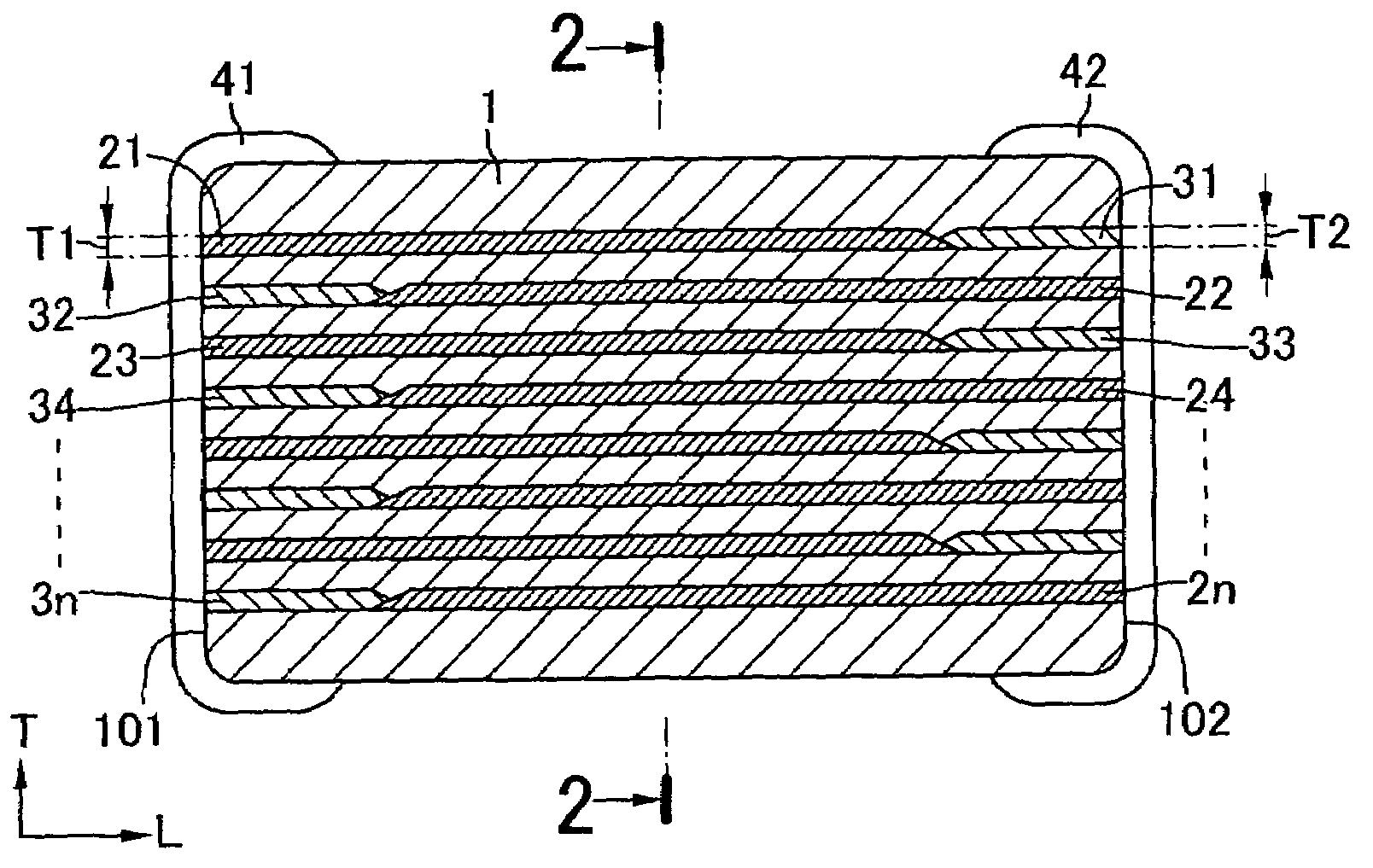
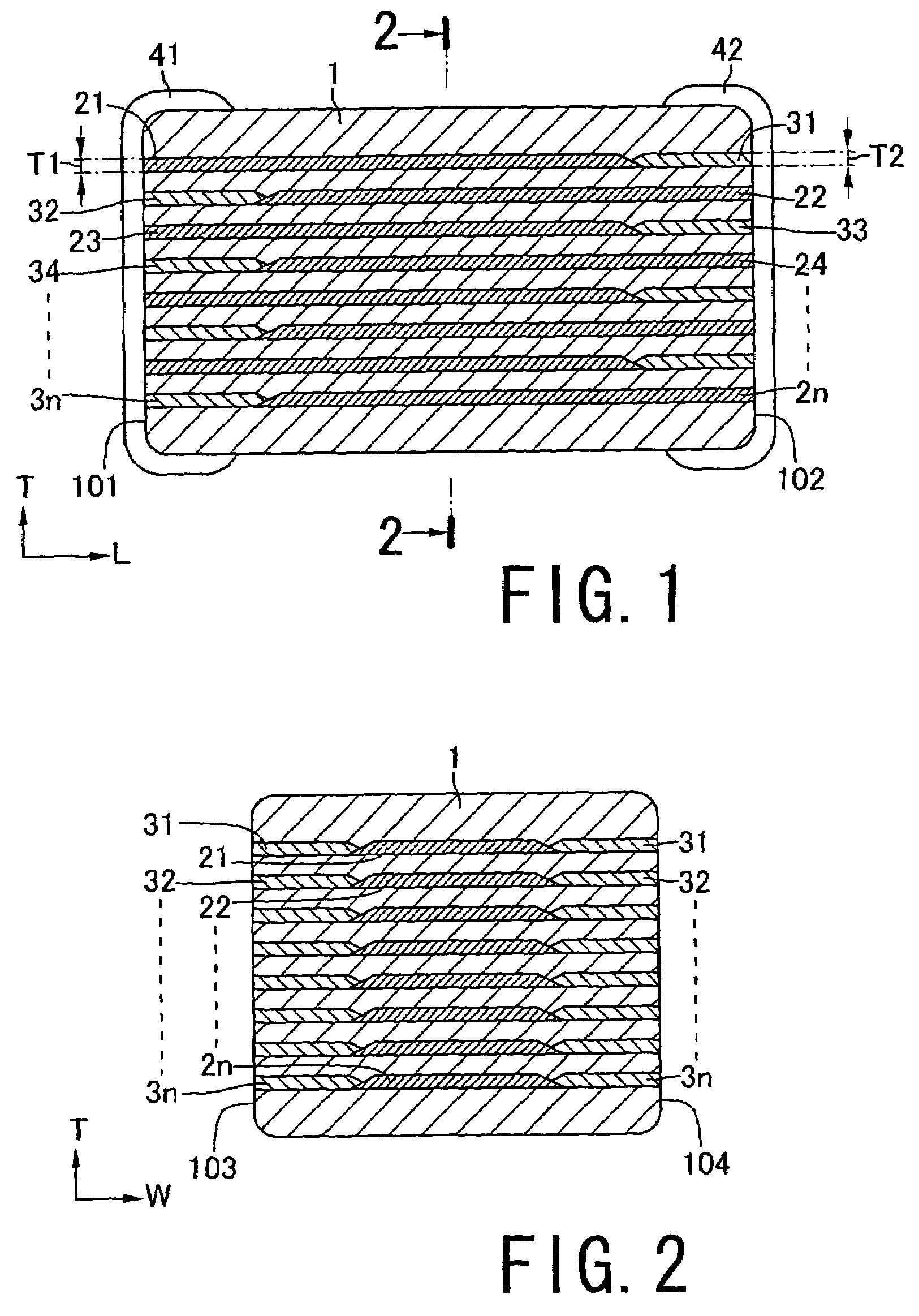
[0032]FIG. 1 is a cross-sectional view showing an embodiment of a multilayer electronic component according to the present invention, and FIG. 2 is an end elevational view taken along a line 2-2 in FIG. 1. An illustrated multilayer electronic component includes a dielectric substrate 1 and n internal electrode layers 21 to 2n. In the illustrated embodiment, the present invention is applied to a multilayer ceramic capacitor, but it can be likewise applied to any other multilayer electronic component such as a multilayer inductor.

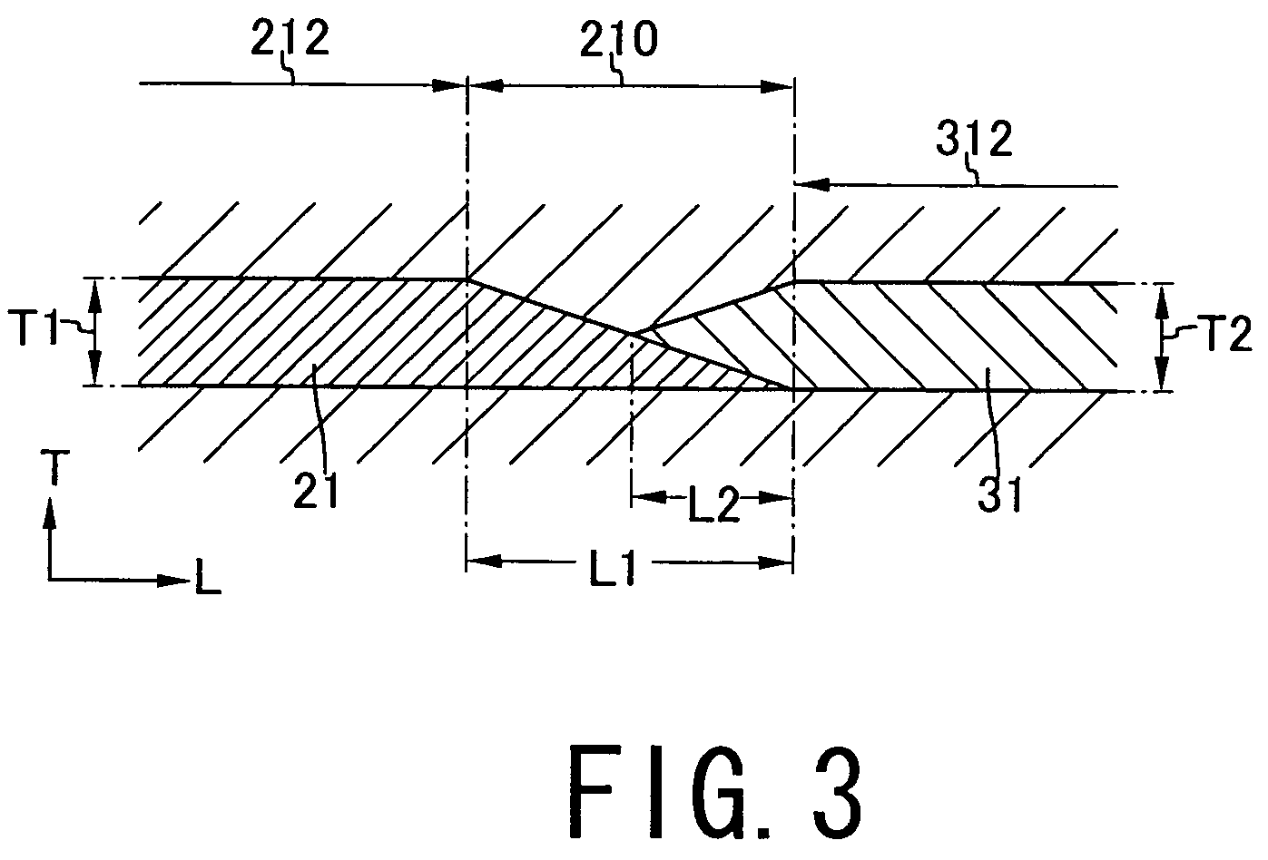
[0033]The dielectric substrate 1 is formed of a dielectric material mainly containing, e.g., barium titanate. The dielectric substrate 1 has a substantially rectangular parallelepiped shape having a length direction L, a width direction W and a thickness direction T, and terminal electrodes 41 and 42 are provided on both end faces 101 and 102 as seen from the length direction L. Each of the terminal electrodes 41 and 42 can be constituted of a multilayer stru...


PUM


Abstract

Internal electrode layers are superimposed in a dielectric substrate 1 at intervals. Step absorption layers are respectively provided on lateral sides of the internal electrode layers. A side portion of the internal electrode layer forms an inclined surface, and the step absorption layer is superimposed so as to partially overlap the inclined surface of the internal electrode layer. This is also applied to the other internal electrode layers and step absorption layers.

Description

BACKGROUND OF THE INVENTION[0001]1. Field of the Invention[0002]The present invention relates to a multilayer electronic component and a manufacturing method thereof.[0003]2. Description of the Related Art[0004]In general, a multilayer electronic component such as a multilayer ceramic capacitor is made of a sheet laminated body formed by superimposing a plurality of ceramic green sheets each including an internal electrode.[0005]In such a multilayer electronic component, a step generated with respect to another part due to a thickness of the internal electrode cannot be ignored as the number of laminated layers is increased. That is, a step due to presence / absence of the internal electrode is produced between a lamination region including a margin portion on which the internal electrode is not printed and a lamination region including the internal electrode. Such a step induces a crack or delamination at the time of baking, which can be a factor of deteriorating characteristics of a...

Claims


Application Information

Patent Timeline
Patent Type & Authority Patents(United States)
IPC IPC(8): H01G4/228
CPCH01G4/30H01G4/012B63B39/06B63B43/02B63B43/18B63B59/02B63B2039/067B63B2041/003B63B2221/20B63B2231/04
Inventor KOJIMA, TATSUYAUEDA, KANAMETONOGAI, TORUMASAOKA, RAITAROIWASAKI, AKINORIYAMAGUCHI, AKIRAMUROSAWA, SHOGO
Owner TDK CORPARATION
Why Eureka
Try Eureka