Si nanowire substrate, method of manufacturing the same, and method of manufacturing thin film transistor using the same

a technology of nanowires and substrates, applied in the direction of crystal growth process, transportation and packaging, chemistry apparatus and processes, etc., can solve the problems of many impurities in nanowires grown by such a method, difficult and complicated methods of manufacturing nanowires, and low mobility and uniformity of polycrystalline silicon compared to single crystalline silicon, etc., to achieve the effect of simple silicon nanowire film manufacturing process

Active Publication Date: 2007-11-20
SAMSUNG ELECTRONICS CO LTD
View PDF2 Cites 33 Cited by
  • Summary
  • Abstract
  • Description
  • Claims
  • Application Information

AI Technical Summary

Benefits of technology

[0013]According to an example embodiment of the present invention, there is provided a method of manufacturing a silicon nanowire substrate, including preparing a substrate, forming an insulating film on the substrate, forming a silicon film on the insulating film, patterning the insulating film and the silicon film into a strip shape, reducing the line-width of the insulating film by undercut etching at least one lateral side of the insulating film, and forming a self-aligned silicon nanowire film on the upper surface of the insulating film by melting and crystallizing the silicon film.
[0017]According to another example embodiment of the present invention, there is provided a method of manufacturing a silicon nanowire substrate, including preparing a single crystalline silicon substrate, forming an insulating film on the single crystalline silicon substrate, exposing the single crystalline silicon substrate by etching a region of the insulating film, forming a silicon crystal seed on the exposed surface of the single crystalline silicon substrate by epitaxially growing silicon, forming a silicon film on the upper surface of the insulating film, patterning the insulating film and the silicon film formed on the insulating film into a strip shape of which one end part contacts the silicon crystal seed, reducing the line-width of the insulating film by undercut etching at least one lateral side of the insulating film and the silicon crystal seed; melting the silicon film formed on the upper surface of the insulating film and the silicon crystal seed, and forming a self-aligned silicon nanowire film on the upper surface of the insulating film by laterally crystallizing the silicon film from the silicon crystal seed.
[0021]According to an example embodiment of the present invention, there is provided a method of manufacturing a thin film transistor, including preparing a substrate, forming an insulating film on the substrate, forming a silicon film on the insulating film, patterning the insulating film and the silicon film into a strip shape, reducing the line-width of the insulating film by undercut etching at least one lateral side of the insulating film, forming a self-aligned silicon nanowire film on the upper surface of the insulating film by melting and crystallizing the silicon film, defining a source region, a drain region, and a channel region on the silicon nanowire film, sequentially forming a gate insulating film and a gate electrode on the channel region, and doping the source and drain regions with a conductive dopant.
[0024]In an example embodiment, the silicon nanowire film manufacturing process may be simpler, and the location of the silicon nanowire film can be readily controlled.

Problems solved by technology

However, poly crystalline silicon has lower mobility and uniformity than single crystalline silicon.
Methods of manufacturing nanowires may be difficult and complicated.
A crystal growth inducing method may be used to grow nanowires, but this method may only provide nanowire crystals grown perpendicular to a substrate, and a nanowire grown by such a method may have many impurities.
In some cases, location control of the nanowire is needed, which conventional methods may have difficulty providing.
However, the conventional lithographic resolution limit is approximately 30 nm.
Therefore, the manufacture of a nanowire having a line-width of 30 nm or less is difficult.

Method used


Image

  • Si nanowire substrate, method of manufacturing the same, and method of manufacturing thin film transistor using the same
  • Si nanowire substrate, method of manufacturing the same, and method of manufacturing thin film transistor using the same
  • Si nanowire substrate, method of manufacturing the same, and method of manufacturing thin film transistor using the same

Examples


Embodiment Construction

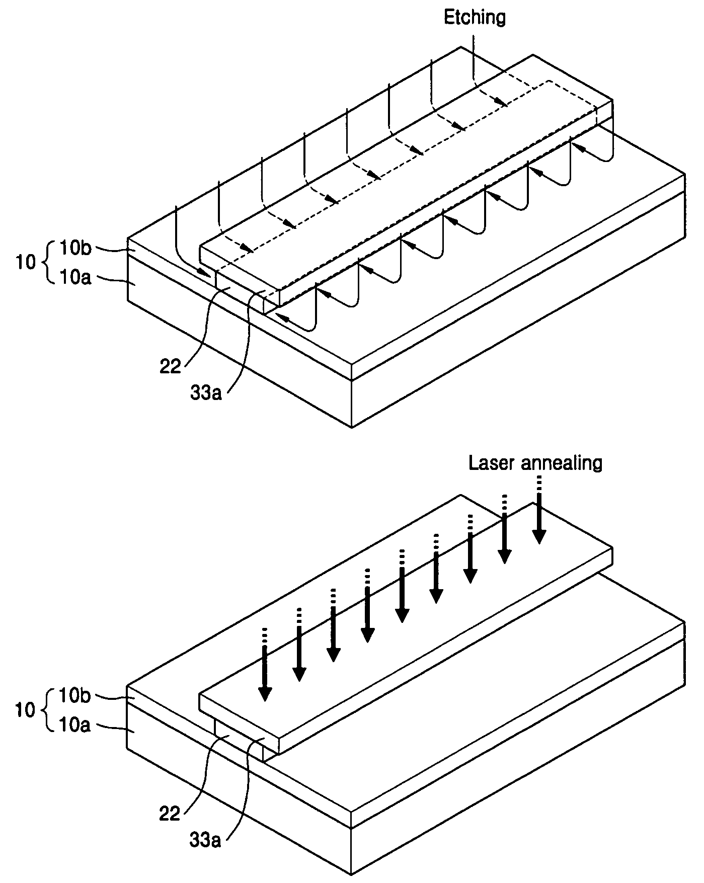
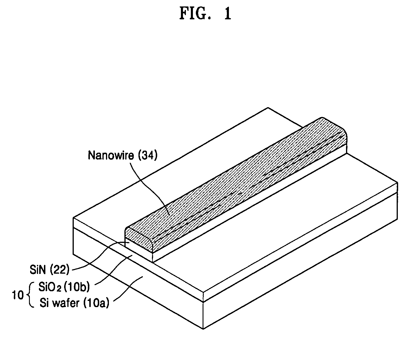
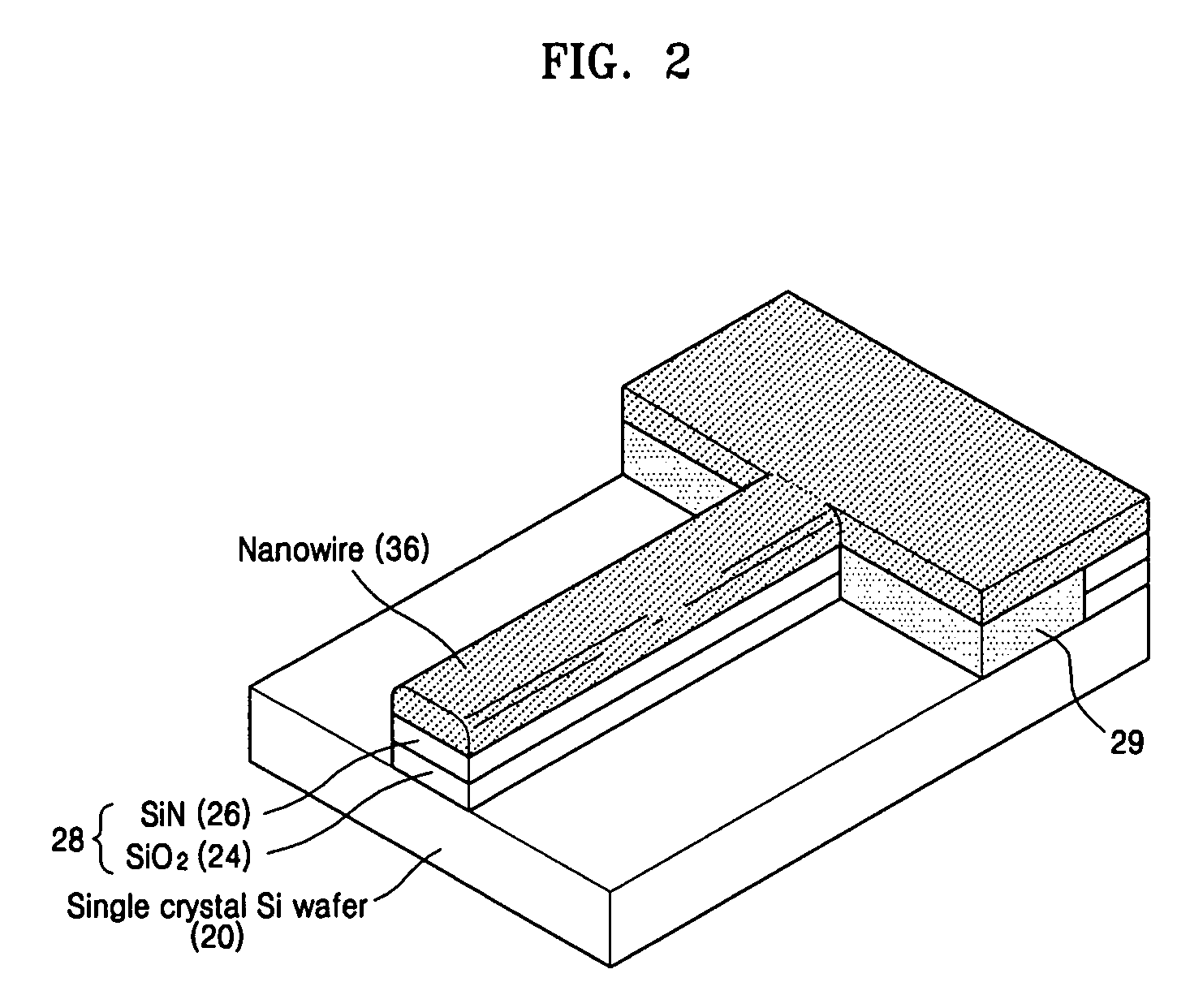
[0032]The present invention will now be described more fully with reference to the accompanying drawings, in which exemplary embodiments of the invention are shown. In the drawings, the thicknesses of layers and regions are exaggerated for clarity.

[0033]Detailed illustrative embodiments of the present invention are disclosed herein. However, specific structural and functional details disclosed herein are merely representative for purposes of describing example embodiments of the present invention. This invention may, however, may be embodied in many alternate forms and should not be construed as limited to only the embodiments set forth herein.

[0034]Accordingly, while example embodiments of the invention are capable of various modifications and alternative forms, embodiments thereof are shown by way of example in the drawings and will herein be described in detail. It should be understood, however, that there is no intent to limit example embodiments of the invention to the particul...


PUM

PropertyMeasurementUnit
line-widthaaaaaaaaaa
lengthaaaaaaaaaa
line-widthaaaaaaaaaa

Abstract

A silicon nanowire substrate having a structure in which a silicon nanowire film having a fine line-width is formed on a substrate, a method of manufacturing the same, and a method of manufacturing a thin film transistor using the same. The method of manufacturing the silicon nanowire substrate includes preparing a substrate, forming an insulating film on the substrate, forming a silicon film on the insulating film, patterning the insulating film and the silicon film into a strip shape, reducing the line-width of the insulating film by undercut etching at least one lateral side of the insulating film, and forming a self-aligned silicon nanowire film on an upper surface of the insulating film by melting and crystallizing the silicon film.

Description

PRIORITY STATEMENT[0001]This application claims the benefit of Korean Patent Application No. 10-2005-0040165, filed on May 13, 2005, in the Korean Intellectual Property Office, the disclosure of which is incorporated herein in its entirety by reference.BACKGROUND[0002]1. Field of the Invention[0003]Example embodiments of the present invention relate to a method of manufacturing a silicon nanowire film, and more particularly, to a silicon nanowire substrate having a structure in which a silicon nanowire film having a fine line-width is formed on a substrate, and a method of manufacturing the same, and a method of manufacturing a thin film transistor using the same.[0004]2. Description of the Related Art[0005]Poly crystalline silicon (poly-Si) may be applied to various electronic devices, for example, flat display devices and solar cells, as a result of having a higher mobility than amorphous silicon (a-Si). However, poly crystalline silicon has lower mobility and uniformity than sing...

Claims


Application Information

Patent Timeline
Patent Type & Authority Patents(United States)
IPC IPC(8): C30B1/02H01L21/20
CPCH01L29/0673H01L29/66772H01L29/78654H01L29/78696Y10T428/26Y10S977/762Y10S977/938Y10S977/814Y10S977/90
Inventor CHO, HANS S.NOGUCHI, TAKASHIXIANYU, WENXUKIM, DO-YOUNGYIN, HUAXIANGZHANG, XIAOXIN
Owner SAMSUNG ELECTRONICS CO LTD
Why Eureka
Try Eureka