Multilayer substrate

a multi-layer substrate and substrate technology, applied in the direction of printed electric component incorporation, semiconductor/solid-state device details, printed element electric connection formation, etc., can solve the problem that the number of layers of the multi-layer substrate cannot be increased, the thickness of the green sheet is not suitable, and the conventional multi-layer substrate fabrication technique cannot accommodate the thickness of the green sheet less than 6 mil, etc. problem, to achieve the effect of accurate control by the user, high purity, and accurate control of dimension shrink

Inactive Publication Date: 2007-11-20
MEDTRONIC MIMIMED INC
View PDF15 Cites 101 Cited by
  • Summary
  • Abstract
  • Description
  • Claims
  • Application Information

AI Technical Summary

Benefits of technology

[0020]Accordingly, it is an object of embodiments of the present invention to provide a multilayer substrate and a method of fabricating a multilayer substrate in which the multilayer substrate may be fabricated without firing. It is also an object of embodiments of the present invention to provide a multilayer substrate and a method of fabricating a multilayer substrate in which the thickness of each layer in the substrate may be widely varied and accurately controlled by the user. It is also an object of embodiments of the present invention to provide a multilayer substrate and a method of fabricating a multilayer substrate in which circuit element and trace tolerance is tightly controlled and dimension shrinkage is kept to a minimum or eliminated altogether. It is also an object of embodiments of the present invention to provide a multilayer substrate fabricated using a process in which dielectrics of high purity may be incorporated into the substrate.
[0028]It is also an object of the present invention to provide a cost-efficient method and apparatus for filling vias in a substrate that reduces or eliminates wasted conductive ink. It is a further embodiment of the present invention to provide a method and apparatus for providing conductive paths through vias in a substrate that are devoid of air, such that the path through the via may be hermetic.

Problems solved by technology

Most conventional multilayer substrate fabrication techniques cannot accommodate green sheets of less than 6 mil thickness because green sheets of these thicknesses tend to be too thin to be successfully fabricated into a multilayer substrate.
Thus, where a multilayer substrate having thin layers is desired, green sheets are generally not feasible as an option.
Also, because the end user has no control over the thickness of each individual green sheet, the end user is forced to limit the number of layers of the multilayer substrate according to the maximum height allowable for the intended application of the multilayer substrate device.
For applications requiring minimum substrate height, the number of green sheets available for lamination may be limited due to their predetermined thickness, thus limiting the complexity of the design.
Accordingly, for small footprint devices that require complex designs, laminated green sheets may prove inadequate.
Another disadvantage of using laminated green sheets for multilayer substrate fabrication is that the green sheets must be sintered, or fired during the fabrication process.
As is the case with many physical processes requiring the introduction of heat, firing the laminated green sheet, i.e., heating the green sheet, causes shrinkage in the various elements of the substrate, including the circuit traces printed on each laminate.
Moreover, the exact amount of shrinkage during firing may be difficult to control.
For designs in which geometries are critical, requiring minimum variance in trace tolerances and high accuracy in trace dimensions or other substrate parameters, laminated green sheets may prove wholly inadequate.
Another disadvantage of using laminated green sheets for multilayer substrate fabrication is that the dielectric used to form the green sheets is generally not of as high a quality as is required for some applications.
These impure dielectrics can be limiting when forming circuit elements, such as high voltage capacitors for example.
Thus, in applications where pure dielectrics are required, the temperature processing required for multilayer substrates fabricated using green sheets generally precludes green sheets as an option for forming such substrates.
However, multilayer substrates formed from thick film processes suffer from many of the same disadvantages as green sheet multilayer substrates.
Excessive cumulative substrate height may be an unacceptable design restriction and, thus, thick film processes may be inadequate for forming multilayer substrates in the intended application.
Because thick film processes require firing each substrate layer, multilayer substrates formed using thick film processes also suffer from shrinkage issues.
Like green sheets, designs requiring minimum variance in substrate parameter tolerances and high accuracy in substrate parameter dimensions may not be adequately served by thick film multilayer substrate formation processes.
When conductive ink is pulled through a via, much of the ink is lost due to waste.
However, for large production runs, the cost attributed to wasted ink could ultimately exceed the cost of the substrate itself.
Thus, for large production runs, filling substrate vias using vacuum techniques becomes cost prohibitive.
Although there is less waste in thick film techniques, traditional squeegee via filling techniques typically allow air to be trapped in the conductive ink, causing air voids to form within the interior of the via.
Air voids are deleterious to the conductive path through the via, plaguing the via with a variety of performance detractors.
If an implantable device is formed having vias that require hermetic sealing, any air voids within the via that compromise the hermeticity of the path and allow fluids to pass through the via could result in device malfunction or even device failure, which could have disastrous consequences for the user of the device.

Method used


Image

  • Multilayer substrate
  • Multilayer substrate
  • Multilayer substrate

Examples


Embodiment Construction

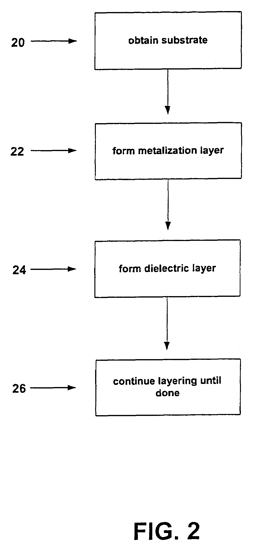
[0046]In the following description of preferred embodiments, reference is made to the accompanying drawings which form a part hereof, and in which are shown by way of illustration specific embodiments in which the invention may be practiced. It is to be understood that other embodiments may be utilized and structural changes maybe made without departing from the scope of the preferred embodiments of the present invention.

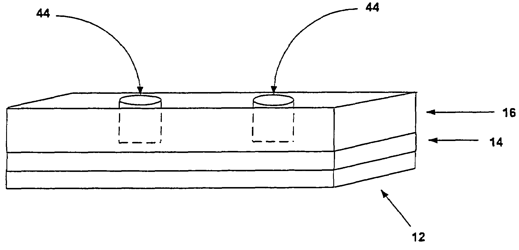
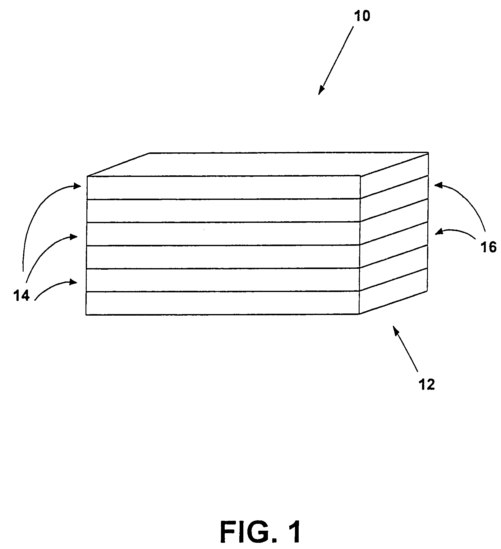
[0047]A multilayer substrate 10 according to an embodiment of the present invention is shown generally in FIG. 1. The multilayer substrate 10 may contain a plurality of alternating dielectric layers and conductive layers. As shown in FIG. 1, the multilayer substrate 10 starts with a base substrate 12, on top of which is a metalization, or conductive, layer 14. The multilayer substrate 10 of FIG. 1 includes two other metalization layers 14. Sandwiched in between the metalization layers 14 are dielectric layers 16.

[0048]The base substrate layer 12 may be rigid or flex...


PUM


Abstract

A multilayer substrate device formed from a base substrate and alternating metalization layers and dielectric layers. Each layer is formed without firing. Vias may extend through one of the dielectric layers such that two metalization layers surrounding the dielectric layers make. contact with each other. The vias may be formed by placing pillars on top of a metalization layer, forming a dielectric layer on top of the metalization layer and surrounding the pillars, and removing the pillars. Dielectric layers may be followed by other dielectric layers and metalization layers may be followed by other metalization layers. Vias in the substrate may be filled by forming an assembly around the substrate, the assembly including printing sheets containing a conductive ink and pressure plates for applying pressure. A vacuum may be applied to remove air in the ink. Pressure may then be applied to the printing sheets through the pressure plates. The conductive ink in the printing sheets is pushed through the vias when pressure is applied by the pressure plates.

Description

CROSS-REFERENCE TO RELATED APPLICATIONS[0001]This application is a divisional of application Ser. No. 10 / 331,186 filed Dec. 26, 2002, which is in turn claims the benefit of prior filed U.S. Provisional Patent Application No. 60 / 414,289; filed Sep. 27, 2002. The entirety of each which are incorporated herein by reference.BACKGROUND[0002]1. Field of the Invention[0003]The present invention relates to the field of semiconductor fabrication technology and, in particular, to the formation of substrates having multiple layers, i.e., the formation of multilayer substrates.[0004]2. Description of Related Art[0005]Multilayer substrates are becoming increasingly popular in the microelectronics arena for a variety of reasons. The high packing densities, accommodation of varied types of circuit elements and facilitation of complex circuitries afforded by multilayer substrates have generated an increased interest and use in these devices. As the requirements for increased packing densities, comp...

Claims


Application Information

Patent Timeline
Patent Type & Authority Patents(United States)
IPC IPC(8): H01L21/4763H01L21/48H05K1/16H05K3/04H05K3/40H05K3/46
CPCH01L21/4857H05K3/4061H05K3/4667H05K3/467H05K1/092H05K3/4647H01L2924/0002H05K2201/0179H05K2203/0278H01L2924/00
Inventor SHAH, RAJIVPENDO, SHAUNBABIRICKI, EDWARD G.
Owner MEDTRONIC MIMIMED INC
Why Eureka
Try Eureka