Solid-state image pickup element and method of producing the same
a pickup element and solid-state technology, applied in the direction of radio frequency control devices, instruments, television systems, etc., can solve the problems of difficult to form thin metal film on the tapered face with high controllability, difficult to maintain a high sensitivity, and difficult to guide oblique incident light to the photodiode, etc., to achieve the effect of reducing the number of production steps
- Summary
- Abstract
- Description
- Claims
- Application Information
AI Technical Summary
Benefits of technology
Problems solved by technology
Method used
Image
Examples
embodiment 1
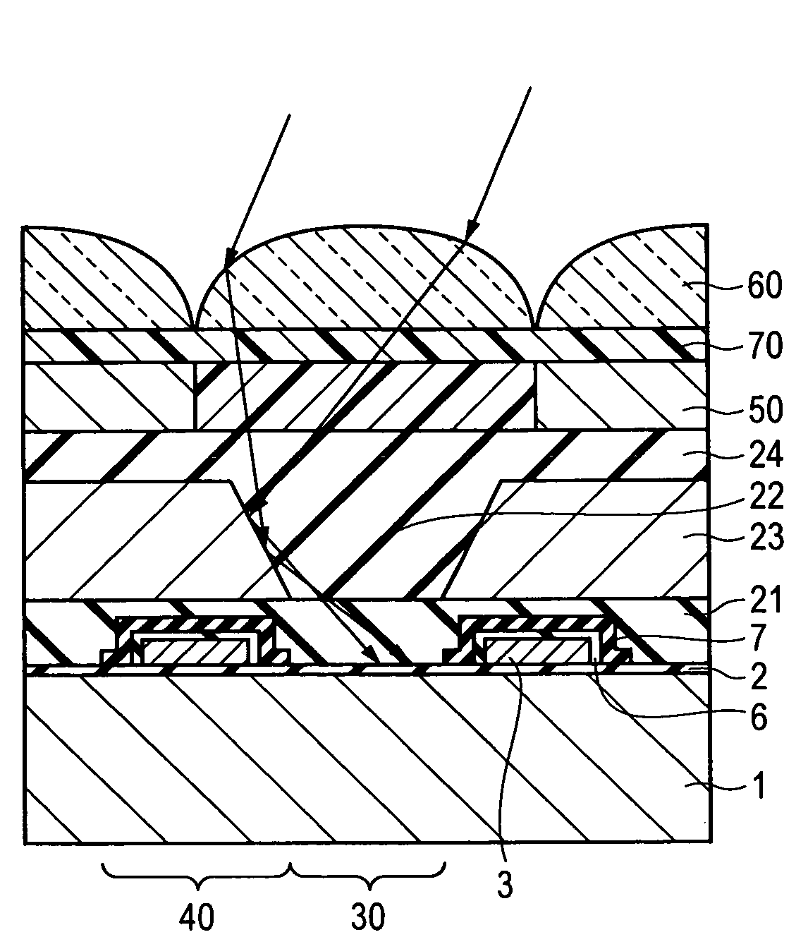
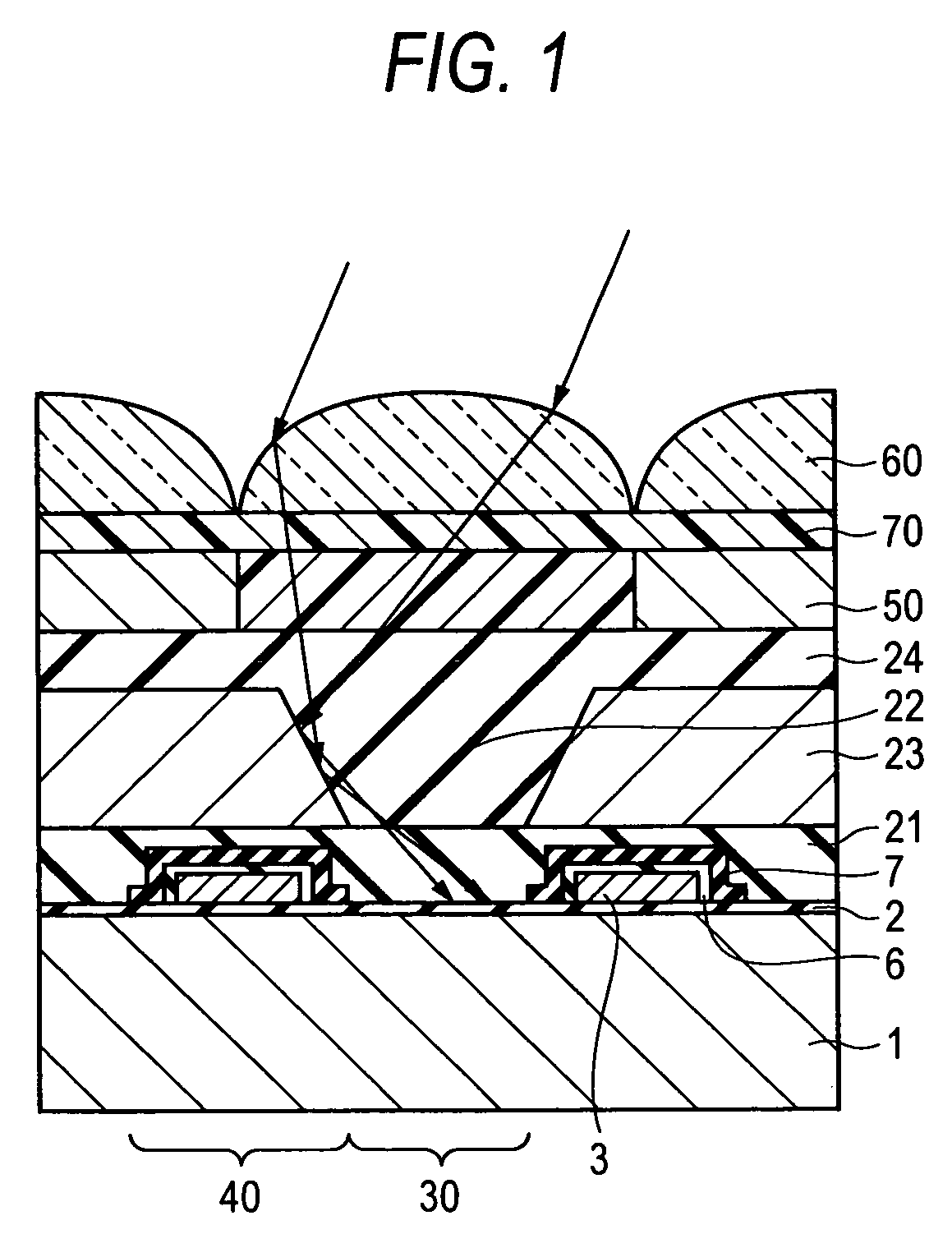
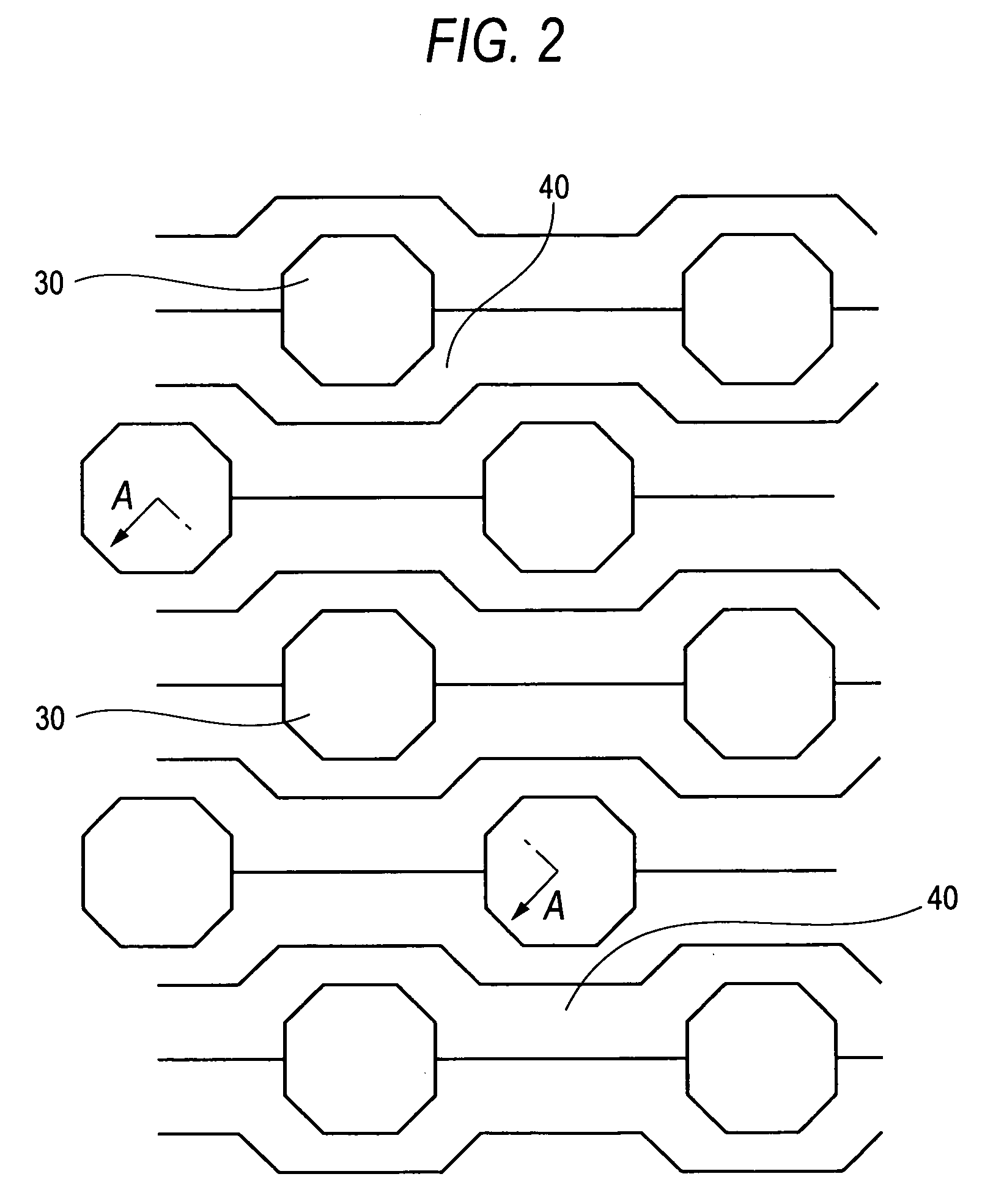
[0067]FIG. 1 is a section view showing a main portion of a solid-state image pickup element, and FIG. 2 is a plan view of a main portion of an imaging region. FIG. 1 is a section view taken along the line A-A of FIG. 2. The solid-state image pickup element is characterized in that an optical waveguide 22 formed above a photodiode 30 serving as a photoelectric converting portion is formed in a reflective material film 23 which covers the surface of a semiconductor substrate, and which has a hole portion on the photodiode 30. The hole portion configures a tapered face that is opened toward an upper portion of the semiconductor substrate, so as to further enhance the light converging property. The reflective material film 23 is configured by a single-layer film of aluminum.
[0068]The reflective material film 23 configured by the aluminum film in which an opening is formed in a region corresponding to the photodiode 30 is disposed above an imaging section of the solid-state image pickup ...
embodiment 2
[0089]Next, Embodiment 2 of the invention will be described.
[0090]As described in Embodiment 1 above, the embodiment characterized in that the reflective material film 23 is formed in the same step as a wiring layer 23e which is made of an aluminum layer in a peripheral circuit section as shown in FIG. 5.
[0091]The embodiment is generally identical with Embodiment 1. In the embodiment, however, a charge transferring portion and a photodiode are formed in the substrate. The left side of the break line shows the peripheral circuit section, and the right side shows the imaging section.
[0092]The reflective material film 7 which is configured by a tungsten film, and in which an opening is formed in a region corresponding to the photodiode 30 is disposed above the imaging section of the solid-state image pickup element. On the film, the reflective material film 23 which is configured by an aluminum layer, and in which an opening is formed correspondingly with the photodiode 30 is formed ov...
PUM
 Abstract
Description
Claims
Application Information


