Optical device and apparatus comprising the optical device

a technology of optical devices and optical components, applied in the field of optical devices, can solve the problems of deteriorating the advantage of utilization, poor appearance, and deteriorating the use efficiency of light, and achieve the effect of obtaining the positional accuracy of the light reflecting member

Inactive Publication Date: 2007-11-27
ORMON CORP
View PDF3 Cites 139 Cited by
  • Summary
  • Abstract
  • Description
  • Claims
  • Application Information

AI Technical Summary

Benefits of technology

[0015]It is a second object of this invention to improve the use efficiency of the light emitted from a solid light emitter such as a light emitting diode.
[0045]In a light emission method according to this invention, the light deviated from a predetermined front area among the light emitted from a light source is almost totally reflected by a resin boundary surface, and the light totally reflected by the resin boundary surface is emitted forward by the light reflecting member disposed behind the resin boundary surface. According to this light emission method, the light deviated from the predetermined area is reflected by the resin boundary surface and the light reflecting member in a light path emitted from the light source, thereby realizing a desired directivity pattern by the configurations of the resin boundary surface and the light reflecting member.

Problems solved by technology

In a conventional light emission source in which a light emitting diode is sealed in a mold resin, light emitted from the light emitting diode to its front is emitted from the light emission source as it is, but light emitted in a diagonal direction from the light emitting diode is totally reflected on a boundary surface of the mold resin and scattered in an inside wall of a housing to be lost, resulting into deterioration of use efficiency of light.
This conventional light emission source, however, has the disadvantage that light reflected by the light reflecting member is obstructed by the light emitting diode and the lead frames when it is emitted forward, thereby producing shadows of these components and deteriorating the advantage of utilization of light near the optical axis center where quantity of light should be provided most well.
Furthermore, because of darkness near the optical axis center in the directivity pattern of light emitted by the light emission source, its appearance is bad as a light source for a display, and its visual performance also is bad.
Moreover, just one light emission source becomes so-called point light source, so that the light emission area cannot be enlarged.
However, this approach to increase the chip area of the photo detector reduces the number of chips which can be taken from one piece of monocrystal wafer, resulting into large increase of the manufacturing cost.

Method used


Image

  • Optical device and apparatus comprising the optical device
  • Optical device and apparatus comprising the optical device
  • Optical device and apparatus comprising the optical device

Examples


tenth preferred embodiment

[0195]FIG. 16 is a sectional view of a light emission source 30 according to a tenth preferred embodiment. In the light emission source 30 of this embodiment, a lens configuration of a lens-shaped direct emission region 18 is formed to be a Fresnel lens to decrease the thickness of the direct emission region 18 or the light emission source 30.

eleventh preferred embodiment

[0196]FIG. 17 is a sectional view of a light emission source 31 according to an eleventh preferred embodiment. In the light emission source 31 of this embodiment, a rear face of a mold resin 13 is formed to include a Fresnel lens on a surface of which a light reflecting portion 20 is formed. In this embodiment, the thickness of the light emission source 31 can be reduced.

twelfth preferred embodiment

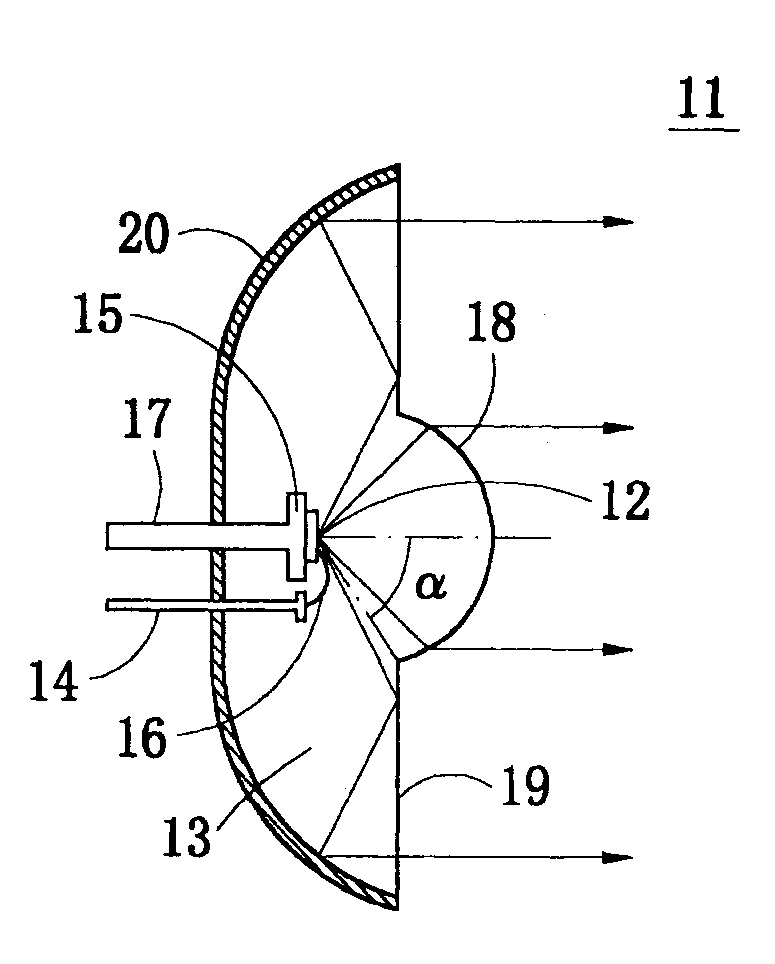
[0197]FIG. 18 is a sectional view of a light emission source 32 according to a twelfth preferred embodiment. In this embodiment, a mirror 33 is disposed near a light emitter 12 within a mold resin 13 so as to reflect the light emitted sideway from the light emitter 12 toward a total reflection region 19. The light reflected by the mirror is totally reflected by the total reflection region 19, and further reflected by a light reflecting member 20 to be emitted forward from the total reflection region 19. If desired, the mirror 33 may be formed on an inner wall of a stem 15 (see FIG. 24).

[0198]According to this embodiment, the light emitted sideway in the light emitted from the light emitter 12 is directly reflected by the light reflecting portion 20 to be avoided from becoming lost light, whereby the light emitted in a side direction is effectively used and the use efficiency of light emitted from the light emitter 12 is further improved.


PUM


Abstract

On a front wall of a mold resin (13) sealing a light emitter (12), a direct emission region (18), through which the light emitted from the light emitter (12) directly passes to the outside, and a total reflection region (19), by which the light emitted from the light emitter (12) is totally reflected, are formed. The direct emission region (18) is formed into a shape of a convex lens. A light reflection portion (20) which is made of a concave mirror is provided on the rear face of the mold resin (13). When a part of the light emitted from the light emitter (12) passes through the direct emission region (18), it is affected by the lens to be emitted to the front direction. After another part of the light emitted from the light emitter (12) is totally reflected by the total reflection region (19), it is reflected by the light reflection portion (20) to be emitted to the front direction through the total reflection region (19).

Description

CROSS-REFERENCE TO RELATED APPLICATION [0001]This application is a continuation of U.S. patent application Ser. No. 10 / 148,242, filed May 29, 2002 now abandoned.TECHNICAL FIELD OF INVENTION[0002]This invention relates to an optical device and an apparatus employing the optical device. More specifically, this invention relates to a light emission source having a solid light emitter such as a light emitting diode, a light receiver having a photo detector such as a photo diode, photo-transistor, a photoelectric transducer (a solar cell) etc., an optical component employing the light emission source and the photo detector, and an optical device including the light emission source, the light receiver, and the optical component. Further, this invention relates to a light emission method, a light incident method and a method for manufacturing an optical component. In addition, this invention relates to a photoelectric sensor employing the optical device, a self light generating apparatus, ...

Claims


Application Information

Patent Timeline
Patent Type & Authority Patents(United States)
IPC IPC(8): F21V7/00F21V5/00F21V7/04H01L33/54H01L33/58H01L33/60
CPCH01L33/60H01L33/54H01L33/58H01L2224/48091H01L2224/48247H01L2924/1815H01L2924/00014H01L31/12
Inventor KIYOMOTO, HIRONOBUHOSOKAWA, HAYAMIYASUDA, NARUHOMMA, KENJITERAKAWA, YUKARI
Owner ORMON CORP
Why Eureka
Try Eureka