LED device and method for manufacturing the same

a manufacturing method and led technology, applied in the manufacture of electrode systems, discharge tubes luminescent screens, electric discharge tubes/lamps, etc., can solve the problems of unstable amount and characteristics of injected resin, difficulty in controlling the amount of first resin and reproducing that amount, and large capacity of fluorescent resin as a whole, so as to improve the accuracy of filling the fluorescent resin with respect to the concave portion. , the effect of small variation of color ton

Inactive Publication Date: 2007-11-27
STANLEY ELECTRIC CO LTD
View PDF28 Cites 6 Cited by
  • Summary
  • Abstract
  • Description
  • Claims
  • Application Information

AI Technical Summary

Benefits of technology

[0020]According to an aspect of the invention an LED device manufacturing method and LED device can be provided that has a small variation in color tone between products, has good efficiency of extracting light from the LED device, and has high luminous intensity.
[0028]Thus, a bonding wire does not obstruct injection of the fluorescent resin and it is therefore possible to consistently encapsulate the LED chip mounted in each concave portion with the resin.
[0029]Moreover, the wavelength conversion material (e.g., fluorescent resin) can diffuse to all the concave portions and the space communicating regions due to its natural flow from at least one space communicating region. Thus, the height of the filled fluorescent resin can become even throughout the concave portions and the space communicating regions. Therefore, it is possible to fill each concave portion with the fluorescent resin in a quantitative manner. Also, the thickness of the fluorescent resin on a light-emitting surface of the LED chip mounted in each concave portion becomes even. Furthermore, it is possible to achieve an LED device having a small variation of color tone of light between products.
[0030]In addition, since the concave portions and the space communicating regions can be connected to one another, the capacity that is filled with the fluorescent resin as a whole is large. Thus, even if an error occurs in the amount of injected fluorescent resin, the error is dispersed throughout the concave portions and the space communicating regions and can have little or no effect on an error of the amount of the resin in each concave portion. That is, accuracy of the filling amount of the fluorescent resin with respect to the concave portion can be easily improved, and accuracy of the filling amount of the fluorescent resin between the concave portions can also be easily improved. Therefore, it is possible to achieve an LED device having a small variation in color tone of light between products and achieve light having a desired color tone in an individual LED device.
[0031]Since the fluorescent resin that is injected into at least one space communicating region can diffuse to all the concave portions and the space communicating regions due to its natural flow, all the concave portions can be filled with the fluorescent resin by one injection operation. Thus, operating efficiency can be improved, resulting in improvement of productivity.
[0032]Furthermore, a condenser made of a transparent resin can be formed above the concave portion in which the LED chip is mounted. Due to this, light that is emitted from the LED chip and that is radiated to the outside of the LED device (to the air) can be collected in one direction so as to increase the luminous intensity of the LED device on its optical axis. It is also possible to easily obtain a desired light distribution property.

Problems solved by technology

In this case, however, the amount of the first resin in the concave portion is very small and therefore it is difficult to control the amount of the first resin and to reproduce that amount.
Thus, the bonding wire obstructs the resin discharged from the nozzle of the device, making injection of the resin unstable.
Therefore, the amount and characteristics of the injected resin are unstable.
Thus, it is difficult to disperse the fluorescent material uniformly in the encapsulating resin.
Moreover, it is also difficult to consistently achieve a mixing ratio of the transparent resin and the fluorescent material in the encapsulating resin with high precision and high reproducibility.
Accordingly, uniformity of light emitted from the LED to the outside (to the air) is impaired and a tone difference between products can occur.
Thus, a required focusing effect of the lens, or a required light distribution property, can not be obtained.
Thus, injection of the fluorescent resin discharged from the nozzle of the device into the first cup is not assured, because the bonding wire obstructs that injection.
For this reason, the injection amount may not be stable.

Method used


Image

  • LED device and method for manufacturing the same
  • LED device and method for manufacturing the same
  • LED device and method for manufacturing the same

Examples


Embodiment Construction

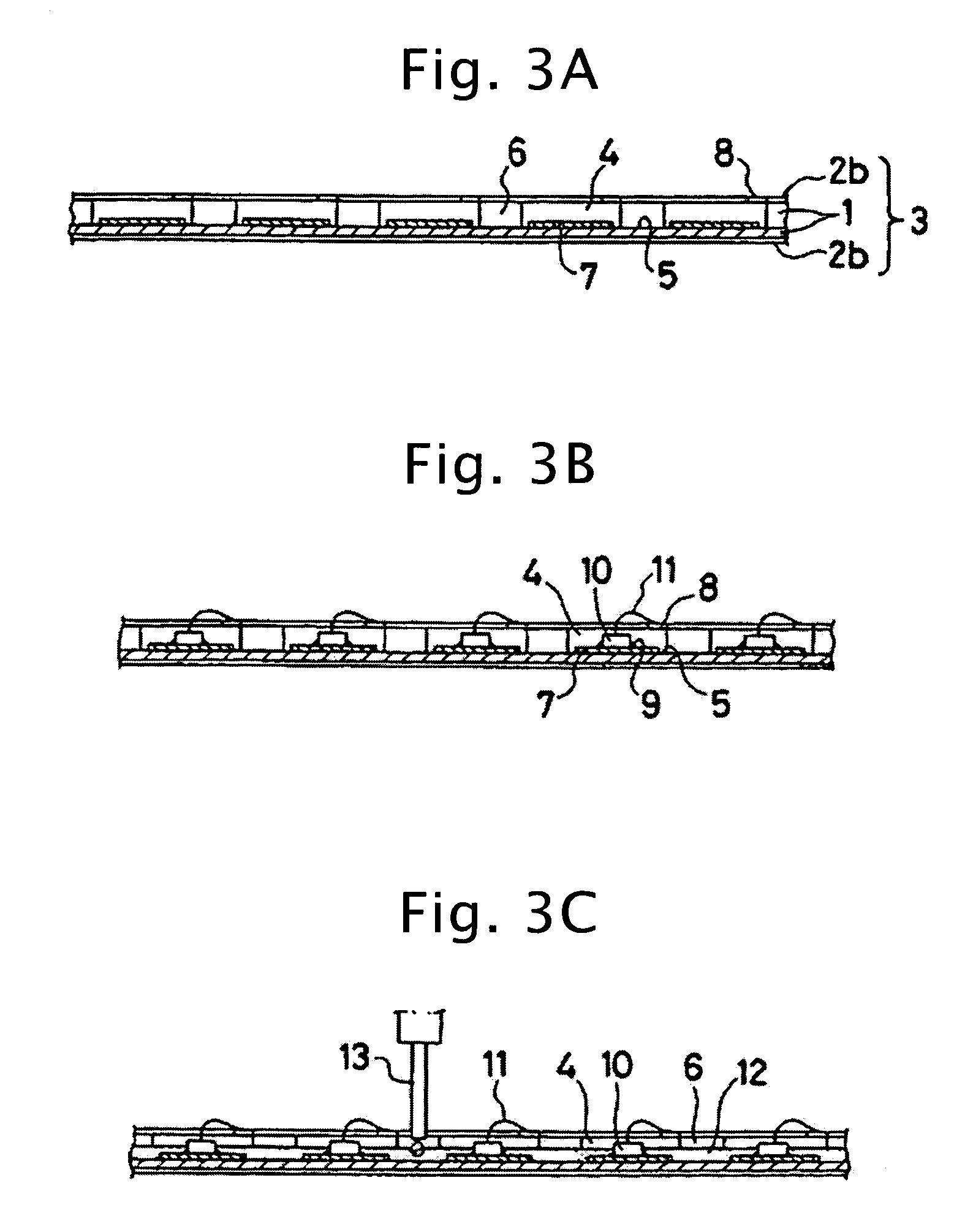
[0039]An exemplary embodiment of the invention will now be described in detail, with reference to FIGS. 3A to 3E, 4A, 4B, and 5 (the same or similar components are labeled with the same reference numerals). The exemplary embodiment to be described hereinafter is an example of the invention, and various technical features are imposed thereon. However, the scope of the invention is not limited to the exemplary embodiment.

[0040]FIGS. 3A to 3E are cross-sectional views showing respective processes of an LED device manufacturing method according to an embodiment of the invention. FIG. 4A is a top plan view corresponding to the process of FIG. 3A and FIG. 4B is a top plan view corresponding to the process of FIG. 3B.

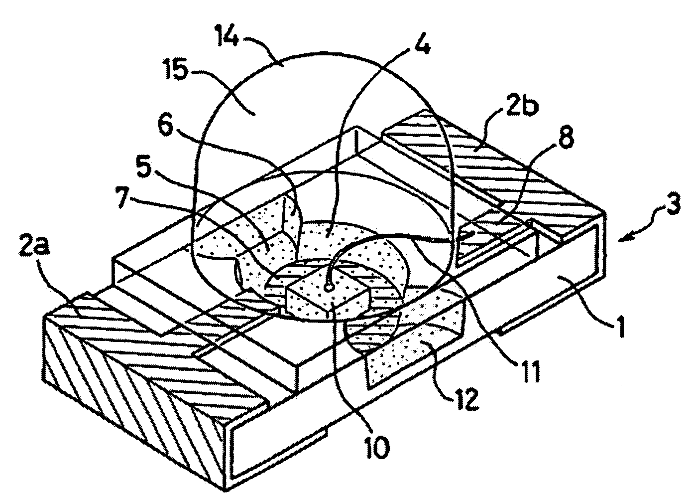
[0041]First, a multiple LED substrate 3 having a plurality of LED device regions is prepared, as shown in FIGS. 3A and 4A. This substrate 3 can include an insulating portion 1 formed by an insulating member and a pair of conductor patterns 2a and 2b. These conductor patterns 2...


PUM

PropertyMeasurementUnit
transparentaaaaaaaaaa
shapeaaaaaaaaaa
color toneaaaaaaaaaa

Abstract

An LED device manufacturing method can produce an LED device that can emit light of a given color tone by additive color mixture of light emitted from an LED chip and light obtained by wavelength conversion of the light emitted from the LED chip. The wavelength conversion can be accomplished by using a wavelength conversion material, such as a fluorescent material. The LED device can have good efficiency of extracting light from the LED and can have high luminous intensity. First cups and second cups can be formed in a substrate including a pair of conductor patterns formed on an insulating portion. The first and second cups can have co-planar bottom surfaces. LED chips can be mounted on die bonding pads that are provided on the bottoms of the first cups. The die bonding pads can be connected to one of the conductor patterns. An upper electrode of each LED chip can be connected to a wire bonding pad extending from the other conductor pattern via a bonding wire. A fluorescent resin containing a transparent resin with a fluorescent material added thereto can be injected into the second cup and then dispersed to fill the first and second cups with the fluorescent resin due to the resin's natural flow. A lens made of a transparent resin can be formed above each LED chip.

Description

[0001]This application claims the priority benefit under 35 U.S.C. § 119 of Japanese Patent Application No. 2004-326276 filed on Nov. 10, 2004, which is hereby incorporated in its entirety by reference.BACKGROUND OF THE INVENTION[0002]1. Field of the Invention[0003]The invention relates to an LED device manufacturing method and LED device. Particularly, the invention relates to a method for manufacturing an LED device and an LED device that emits light of a given color tone by additive color mixture. The additive color mixture includes mixing light emitted directly from an LED chip and light that has been obtained by wavelength conversion of some of the light emitted from the LED chip by use of a wavelength conversion material, e.g., fluorescent material.[0004]2. Description of the Related Art[0005]An LED chip can emit light having a steep spectrum distribution. In order to achieve an LED device for emitting white light using an LED chip as a light source, additive color mixture has...

Claims


Application Information

Patent Timeline
Patent Type & Authority Patents(United States)
IPC IPC(8): H01J9/26H01J9/32H01L33/50H01L33/54H01L33/56H01L33/62
CPCB29C33/0055B29C39/10H01L24/97H01L33/54H01L2224/48465H01L2224/48227H01L2224/48091H01L33/60H01L33/486B29K2995/0026B29L2011/0016H01L2924/00014H01L2924/00H01L2924/12041
Inventor TANAKA, MINORUTANAKA, TOMOHISA
Owner STANLEY ELECTRIC CO LTD
Why Eureka
Try Eureka