Defect size projection

a technology of defect size and projection, applied in the direction of mechanical measuring arrangement, instruments, and mechanical means, can solve the problems of high scattering power of detected defects, measurement becomes nonlinear, and data extrapolation techniques are often difficult to perform in conventional wafer inspection systems, so as to improve the accuracy of defect detection, improve the accuracy of technique, and improve the effect of accuracy

Active Publication Date: 2007-11-27
ADE CORPORATION
View PDF2 Cites 2 Cited by
  • Summary
  • Abstract
  • Description
  • Claims
  • Application Information

AI Technical Summary

Benefits of technology

[0015]According to another aspect of the present invention, an equivalent voltage for a large single defect may be generated by combining the slope value, a predetermined voltage threshold, and an estimate of a defect area at the predetermined voltage threshold. In an illustrative but not necessarily preferred embodiment, the predetermined voltage threshold is an unsaturated voltage threshold. In an illustrative but not necessarily preferred embodiment, the slope value is derived from information taken from another technique for obtaining equivalent voltages for sizing defects and based on Gaussian pulse estimates. The combination of the two defect sizing techniques permits a uniform process to be applied to all defects on a wafer, even when the unsaturated range of the equipment is exceeded. According to an advantage of the present invention, the uniform processobtains equivalent voltages for large size defects. The process can provide sizing for defects directly from voltage associated with the scattering power of the defect over two different defect size ranges. According to another advantage of the present invention, defect sizing determinations can be obtained in a single scan of the wafer. This advantage permits accurate measurements of defects that differ in size by many orders of magnitude without recalibration of the system.
[0016]In accordance with an embodiment of the present invention, a system and method of inspecting semiconductor wafers is provided that is capable of measuring the size and determining the location of a wafer surface defect whether or not the scattering power associated with the defect exceeds the unsaturated range of the system. The semiconductor wafer inspection system includes an optical module including a surface scanning mechanism and a light channel (LC) detector including LC optics. In an illustrative but not necessarily preferred embodiment, the surface scanning mechanism is an acousto-optic deflector (AOD), and the LC optics comprises a quadcell photodetector. The AOD is configured to emit at least one collimated beam of laser light toward a surface of a semiconductor wafer at an oblique angle of incidence θi. The LC optics are configured to detect a light beam specularly reflected from the wafer surface at an angle of reflection θI.
[0017]According to a disclosed embodiment, the size of a defect detected on a semiconductor wafer surface using the surface scanning laser beam is obtained by determining the height of a Gaussian shape representing data collected by the wafer inspection system. The height of a geometric Gaussian shape in three dimensional space is determined by defining an intermediate height of the Gaussian shape, obtaining the cross-sectional area of the Gaussian shape at the intermediate height, determining a value of the cross-sectional area, and combining the cross-sectional area value with a slope value in a predetermined relationship to obtain an equivalent voltage value for the defect. The slope value comprises the slope of a linear relationship between cross-sectional areas of a Gaussian pulse and the natural log of the voltage heights of the pulse at the cross sections. An equivalent voltage amplitude of a large defect can thus be calculated using a relationship between a cross-sectional area at a predetermined cut height, also known here as a height threshold, the height threshold itself, and the slope value. The equivalent voltage amplitude so calculated provides greater accuracy for large defects than a slope estimation technique or the use of the relationship between area at a height threshold and peak voltage or power by themselves.
[0018]According to a feature of the present invention, defect sizing estimates based on three-dimensional Gaussian pulses can be obtained using knowledge of a shape of a beam directed at a wafer and curve fitting techniques to determine a voltage or power equivalent magnitude of a defect. The voltage equivalent magnitude is converted to scattered power produced by the incident beam and then to defect size. When the defect size is very large, the linear relationships relied on can change to include non-linear elements, compromising the accuracy of the technique. When nonlinearities are introduced, such as when non-Gaussian elements and terms become significant in the calculation, an additional technique is used to improve the accuracy of the defect detection, which includes measuring an area of a pulse generated from a defect that has a voltage or power level greater than a predetermined threshold set point. An equivalent power or voltage amplitude is calculated by measuring an area of the pulse at the predetermined threshold set-point. The area is then combined with information based on the slope of a linear relationship between a cross-sectional area of a Gaussian pulse at a predetermined height, and the natural log of the height. The resulting equivalent voltage or power for the defect can then be converted to scattered power, and then defect size to determine the size of the large defect.
[0019]According to another embodiment of the present invention, a method of obtaining the size of a defect detected on a semiconductor wafer surface using the surface scanning laser beam includes determining a slope value m related to the slope of a linear relationship between cross-section area and the natural log of the height of the cross-section in a Gaussian pulse. The slope value m may be a system slope value M that is based in an exemplary embodiment on known characteristics of the defect inspection system such as a spot size of a system laser beam. For example, M can be derived in a system calibration in which
[0020]M=π⁢R12,where R is a positive definite symmetric matrix describing a shape associated with the laser beam. Alternately, or in addition, the slope value may be a measured slope value M that is determined from data representative of area of at least one cross-section in a Gaussian pulse at a selected height and based on the linear relationship between a cross-sectional area and a natural logarithm of a value of a height substantially in accordance with the equation

Problems solved by technology

Such localized light scatters may be indicative of one or more defects on the wafer surface that may render an integrated circuit(s) (IC) fabricated on the wafer to be inoperative.
One drawback of the above-described conventional laser-based surface scanning inspection system is that the maximum scattering power of a detected defect may exceed the dynamic range of the system.
As a result, the electronics within the wafer inspection system may saturate, thereby causing at least some of the defect size measurements performed by the system to be at a power level at which the measurements become nonlinear due to the saturation effects.
However, such data extrapolation techniques are often difficult to perform in conventional wafer inspection systems.
However, conventional algorithms for performing such nonlinear least squares fit techniques often require a significant amount of processing time.
Further, relatively small changes in the data resulting from, e.g., noise or a non-ideal signal, may lead to significantly large changes in the estimated parameters.
There is a drawback to the methodology in that it adds some difficulty because it uses a completely separate calibration process, which can be time consuming and cumbersome.

Method used


Image

  • Defect size projection
  • Defect size projection
  • Defect size projection

Examples


Embodiment Construction

[0034]U.S. Provisional Patent Application No. 60 / 514,289 filed Oct. 24, 2003 entitled EXTENDED DEFECT SIZING and U.S. patent application Ser. No. 10 / 971,694 filed Oct. 22, 2004 of the same title are hereby incorporated herein by reference.

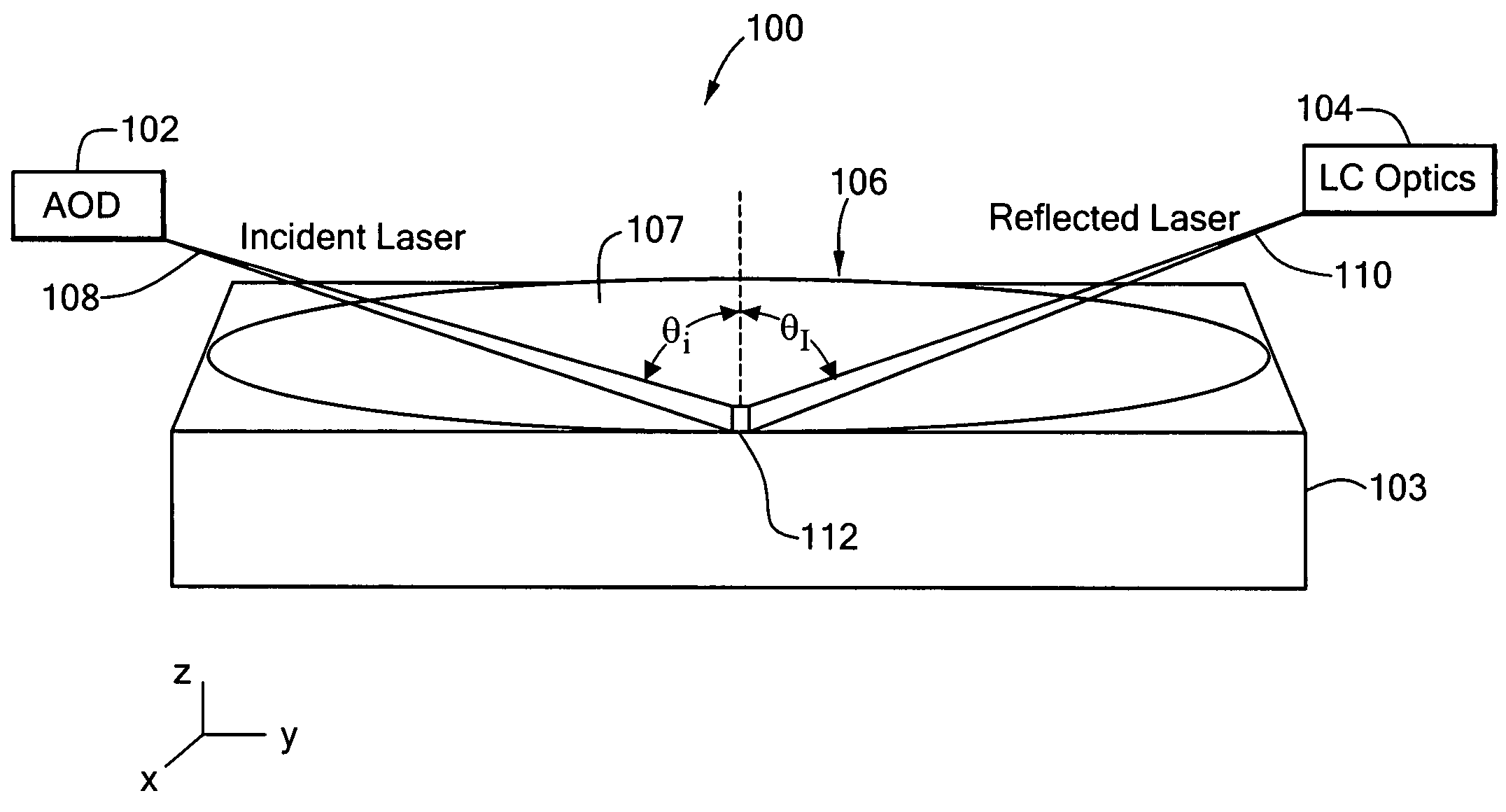
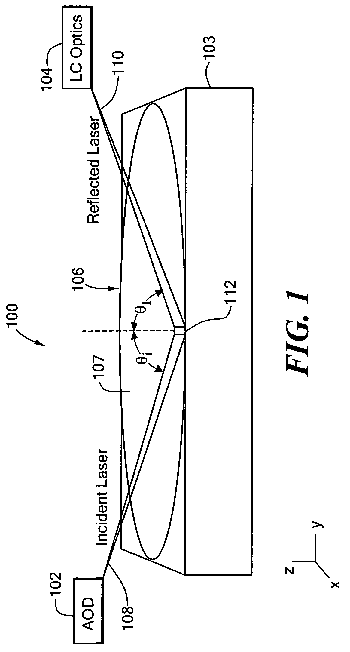
[0035]A system and method of inspecting a semiconductor wafer is disclosed that is capable of measuring the size and determining the location of a defect on a surface of a semiconductor wafer. The presently disclosed wafer inspection system can perform such sizing and locating of wafer surface defects whether or not the scattering power associated with the defect exceeds the dynamic range of the system.

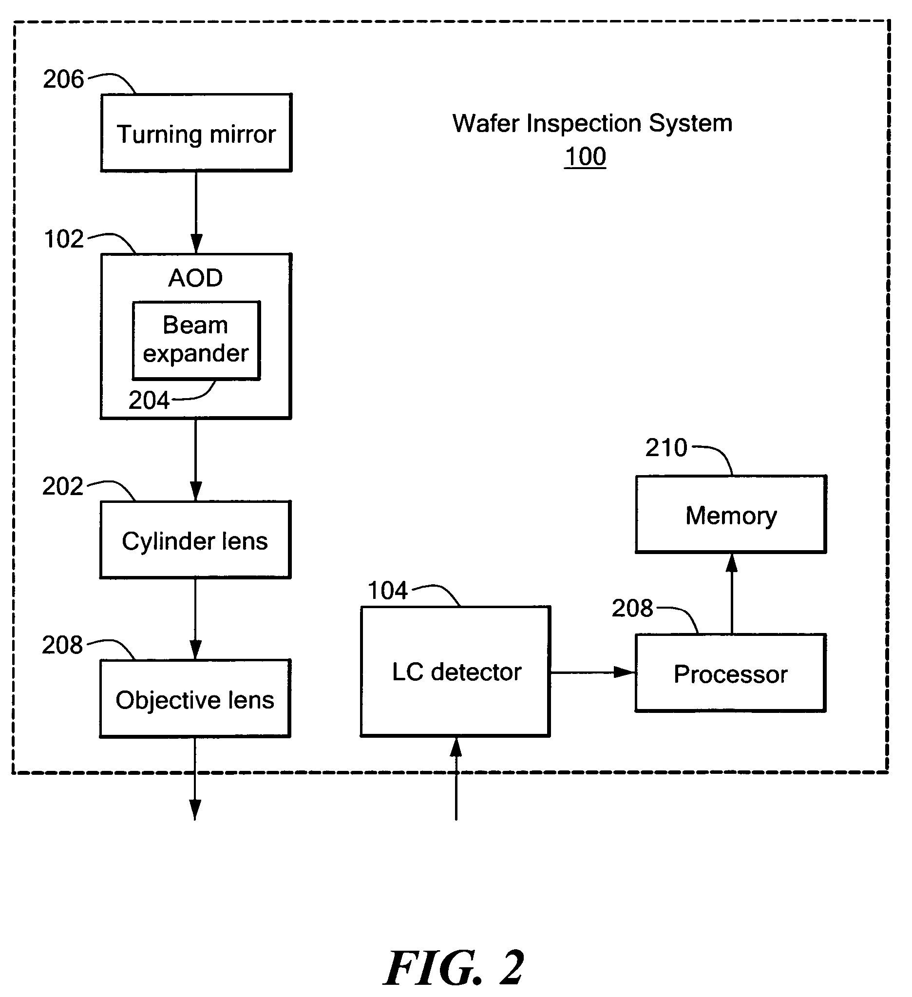
[0036]FIG. 1 depicts an illustrative embodiment of a laser-based wafer surface scanning inspection system 100, in accordance with the present invention. In the illustrated embodiment, the surface scanning inspection system 100 comprises an optical module including a surface scanning mechanism 102, and a light channel (LC) detector including LC optics...


PUM

PropertyMeasurementUnit
angleaaaaaaaaaa
incident angle θiaaaaaaaaaa
diameteraaaaaaaaaa

Abstract

A system and method of inspecting semiconductor wafers that is capable of determining a scattering power associated with a wafer surface defect whether or not the scattering power associated with the defect exceeds the dynamic range of the system. The scattering power of the detected defect is obtained by determining the height of a Gaussian shape representing data collected by the system. The height of the Gaussian shape may be determined by defining a cross-sectional area of the Gaussian shape at an intermediate height, determining a cross-sectional area value and combining the area value, intermediate height and a slope value m that is representative of a relationship between the area of a cross-section in a Gaussian pulse and the height of the pulse at the cross-section. The technique increases the dynamic range of the equipment with a uniform scan process that can determine all defect sizes in a single scan pass.

Description

CROSS REFERENCE TO RELATED APPLICATIONS[0001]This is a Continuation-in-Part application of U.S. patent application Ser. No. 10 / 971,694, filed Oct. 22, 2004 now U.S. Pat. No. 7,184,928 entitled EXTENDED DEFECT SIZING, which claims benefit of U.S. Provisional Patent Application No. 60 / 514,289, filed Oct. 24, 2003, entitled EXTENDED DEFECT SIZING.STATEMENT REGARDING FEDERALLY SPONSORED RESEARCH OR DEVELOPMENT[0002]N / ABACKGROUND OF THE INVENTION[0003]1. Field of Invention[0004]The present invention relates generally to systems and methods of inspecting semiconductor wafers, and relates more specifically to a semiconductor wafer inspection system and method capable of detecting and measuring wafer defects in which the scattering power of the defect exceeds the dynamic range of the system.[0005]2. Description of Related Art[0006]Systems and methods of inspecting semiconductor wafers are known for detecting and measuring defects occurring on a surface of a semiconductor wafer. For example,...

Claims


Application Information

Patent Timeline
Patent Type & Authority Patents(United States)
IPC IPC(8): G01N21/88G01N21/95
CPCG01N21/9501
Inventor JUDELL, NEIL
Owner ADE CORPORATION
Why Eureka
Try Eureka