Semiconductor wafer polishing apparatus, and method of polishing semiconductor wafer

a technology of semiconductor wafers and polishing apparatuses, which is applied in the direction of edge grinding machines, other manufacturing equipment/tools, manufacturing tools, etc., can solve the problems of difficult to suppress the infiltration of abrasives, the loss of yield and/or the apparatus, and the inability to uniformly diffuse gas, etc., to achieve the improvement of the chip yield of the wafer and the operation rate of the individual manufacturing apparatus in the succeeding process step

Inactive Publication Date: 2007-12-04
RENESAS ELECTRONICS CORP
View PDF12 Cites 6 Cited by
  • Summary
  • Abstract
  • Description
  • Claims
  • Application Information

AI Technical Summary

Benefits of technology

[0009]In this semiconductor wafer polishing apparatus, migration of substances between the polishing field and the normal field can be suppressed by forming a curtain of a blown gas. More specifically, by forming the curtain when the circumferential edge side of the wafer is polished by the polishing unit, the abrasive supplied to the polishing unit during polishing and dusts generated during polishing are prevented from infiltration into the normal field. Because the gas herein is blown so as to form the curtain, flow of the gas is relatively stabilized without being destabilized in the gas flow such as in the conventional apparatus based on the single point blowing of the gas.
[0011]As is clear from the above, according to the present invention, the abrasive and the dusts can thoroughly be prevented from adhering onto the circuit-forming region of the wafer, the chip yield of the wafer can be improved, and thereby the operation rates of the individual manufacturing apparatuses in the succeeding process step can be improved.

Problems solved by technology

For this reason, the films easily peels off from the bevel portion and the notch portion of a wafer in diffusion process and those films may adhere onto the top and back surfaces of the wafer, to result in the yield loss and / or the apparatus down.
As a consequence, the gas cannot uniformly be diffused, thereby making it difficult to suppress infiltration of the abrasive by stably spreading the gas over the surface of the wafer.
Blowing from the nozzle only at one point is also highly causative of charge generation on the surface of the wafer, which may degrade the device quality being fabricated on the semiconductor wafer.

Method used


Image

  • Semiconductor wafer polishing apparatus, and method of polishing semiconductor wafer
  • Semiconductor wafer polishing apparatus, and method of polishing semiconductor wafer
  • Semiconductor wafer polishing apparatus, and method of polishing semiconductor wafer

Examples


first embodiment

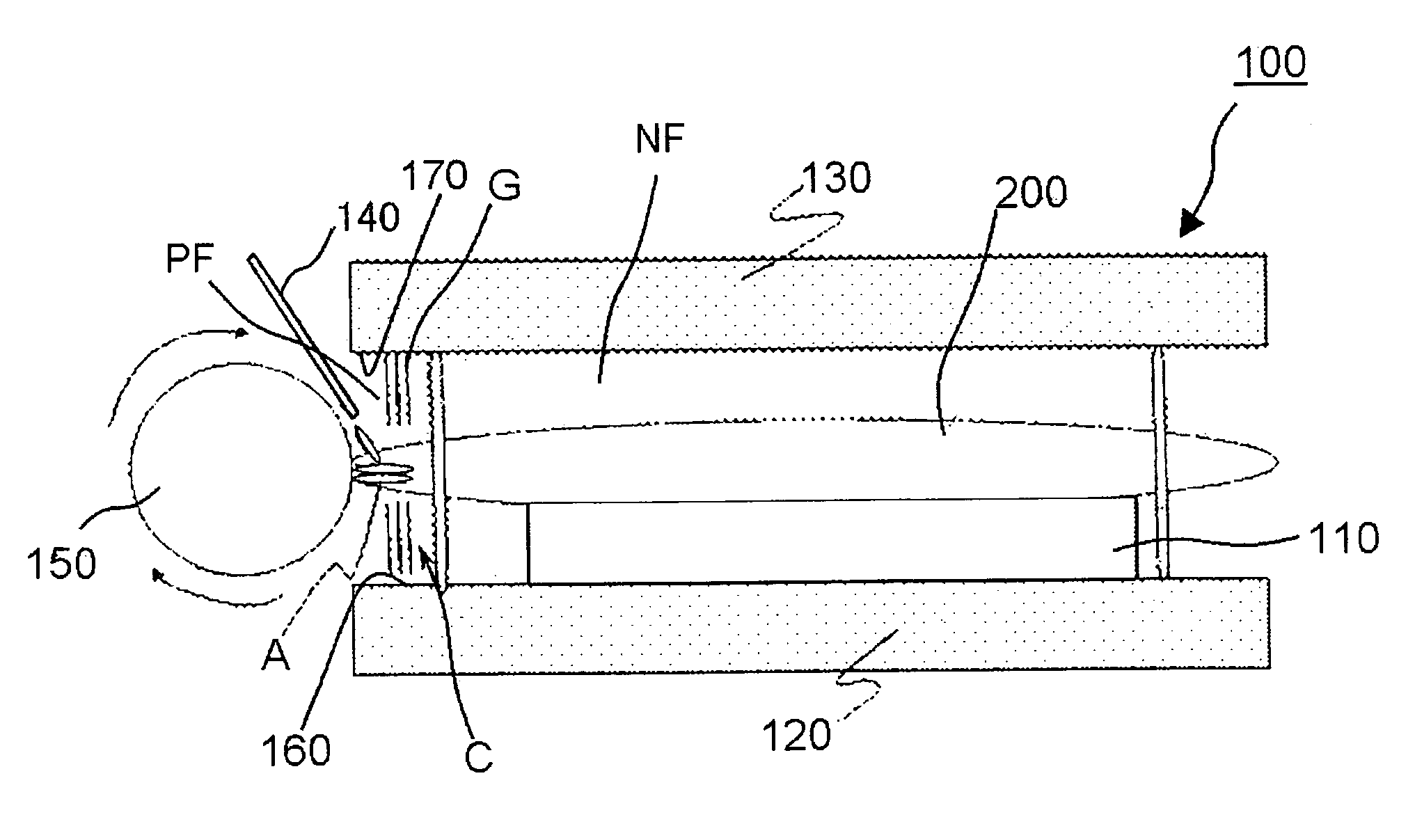
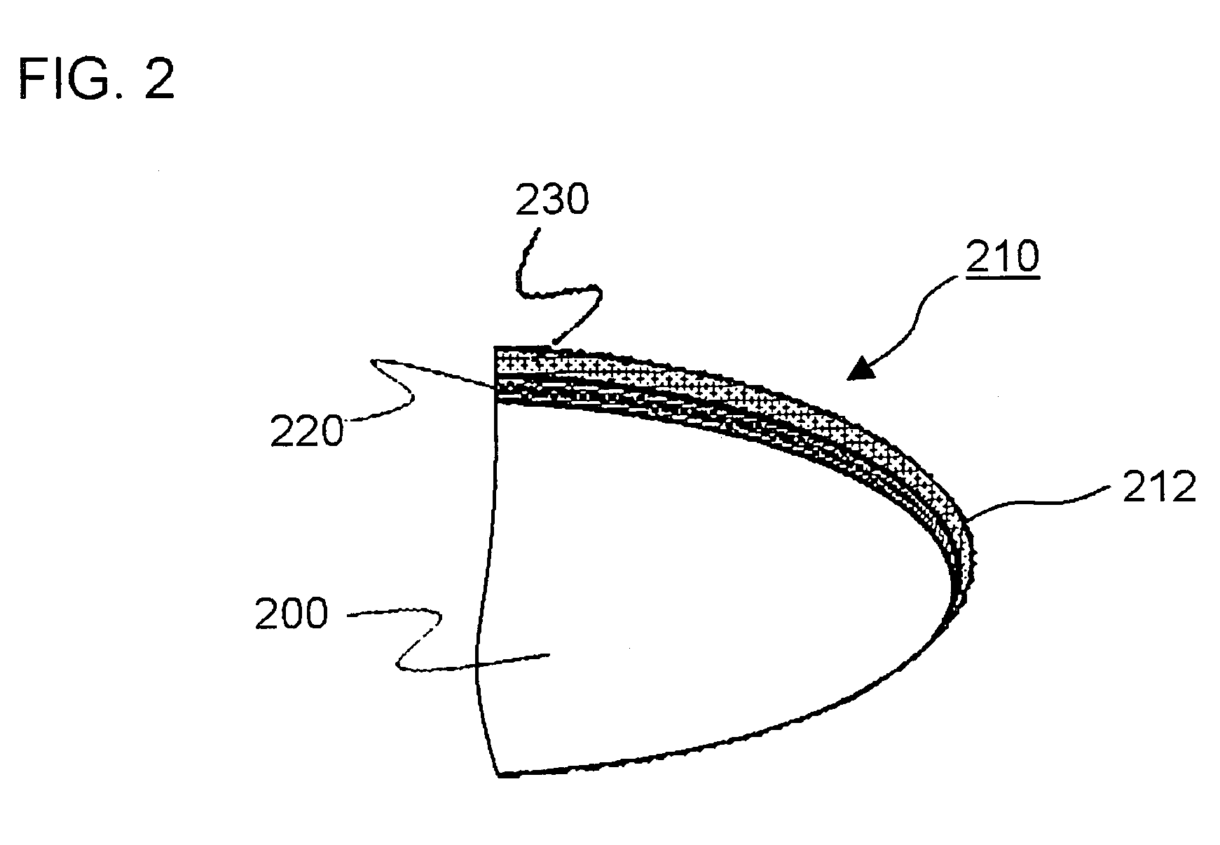
[0026]FIG. 1 to FIG. 8 show the present invention, wherein FIG. 1 is a schematic drawing showing a semiconductor wafer polishing apparatus for polishing a notch portion, FIG. 2 is a drawing explaining the circumferential edge portion of the semiconductor wafer, FIG. 3 is a schematic bottom view of an upper supporting unit of the semiconductor wafer for polishing apparatus polishing the notch portion, FIG. 4 is a sectional view taken along line A-A in FIG. 3, FIG. 5 is a schematic drawing of a semiconductor wafer polishing apparatus polishing a bevel portion, FIG. 6 is a schematic bottom view of an upper supporting unit of the semiconductor wafer for polishing apparatus polishing the bevel portion, FIG. 7 is a sectional view along a line B-B in FIG. 6, and FIG. 8 is a top view of a wafer. It is to be noted that the curtain, shown in FIG. 5 as being illustrated only on the left hand side and on the right hand side for the convenience of explanation, is actually formed so as to surroun...

second embodiment

[0043]FIG. 9 is a bottom view of an upper supporting unit of a semiconductor wafer polishing apparatus according to the present invention.

[0044]The polishing apparatus according to the second embodiment can carry out polishing of both of bevel portion 212 and the notch portion 214 in the same chamber, without transferring the wafer 200 in a cluster-tool. In the polishing apparatus, as shown in FIG. 9, a gas blowing port 470 of an upper supporting unit 430 includes a notch-corresponded portion 472 formed in a near V-shape widened outwardly to the circumferential direction in the bottom view, and a bevel-corresponded portion 474 formed into a ring shape in the bottom view. The unillustrated lower supporting unit is formed with a vertical symmetry with the upper supporting unit 430.

[0045]The wafer 200 is supported in a rotatable manner, wherein the notch portion 214 is polished using the polishing pad 150 while keeping the wafer 200 standing still, and the bevel portion 212 is polished...


PUM

PropertyMeasurementUnit
diameteraaaaaaaaaa
circumferenceaaaaaaaaaa
speedaaaaaaaaaa

Abstract

Aimed at thoroughly preventing abrasive and dusts from adhering onto the circuit-forming region of a wafer, improving yield ratio of semiconductor devices, and thereby improving operation rates of the individual manufacturing apparatuses in the succeeding stage, a semiconductor wafer polishing apparatus of the present invention has a polishing unit polishing the circumferential edge side of a disc-formed wafer; and a gas blowing unit blowing a gas G against the surface of the wafer, so as to separate the space over the wafer by a curtain C of the gas G between a polishing field PF in which the wafer is polished by the polishing unit and a normal field NF except the polishing field PF.

Description

[0001]This application is based on Japanese patent application No. 2005-351240, the content of which is incorporated hereinto by reference.BACKGROUND[0002]1. Technical Field[0003]The present invention relates to a semiconductor wafer polishing apparatus polishing a circumferential edge side of a wafer, and a method of polishing a semiconductor wafer.[0004]2. Related Art[0005]With developing larger scale of integration of circuits, decreasing pattern size and enlarging wafer diameter in semiconductor manufacturing process, a higher chip yield has been desired. One known technique of improving the chip yield ever adopted is to remove an unnecessary portion of films formed on the bevel portion and notch portion of the circumferential edge of a wafer. The bevel portion of a wafer is slightly rounded when one views from the side, and the notch portion of a wafer is near V-shape when one views from the top surface. For this reason, the films easily peels off from the bevel portion and the...

Claims


Application Information

Patent Timeline
Patent Type & Authority Patents(United States)
IPC IPC(8): B24B1/00
CPCB24B9/065
Inventor KUBO, AKIRA
Owner RENESAS ELECTRONICS CORP
Why Eureka
Try Eureka