Method of growing GaN crystal, method of producing single crystal GaN substrate, and single crystal GaN substrate

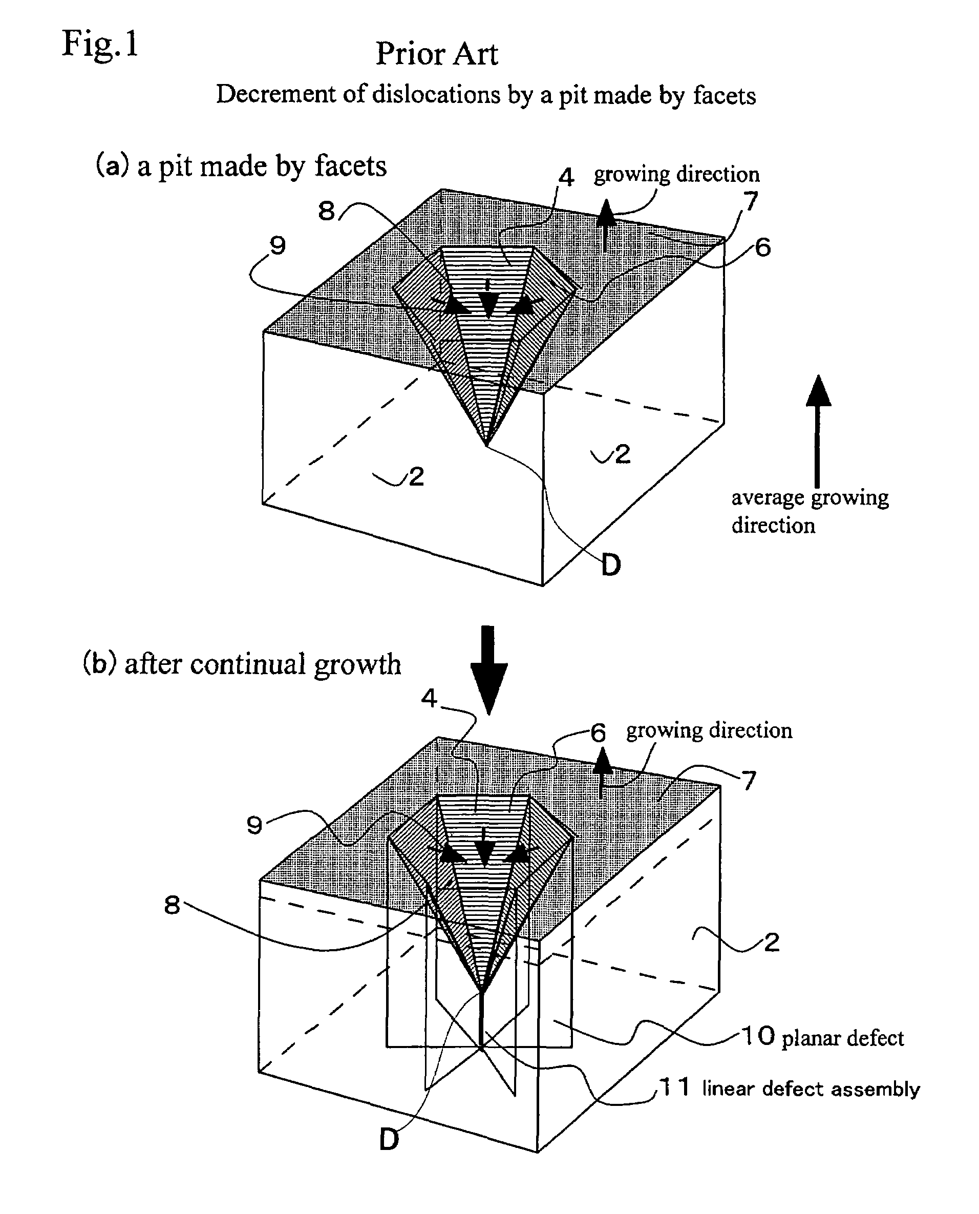
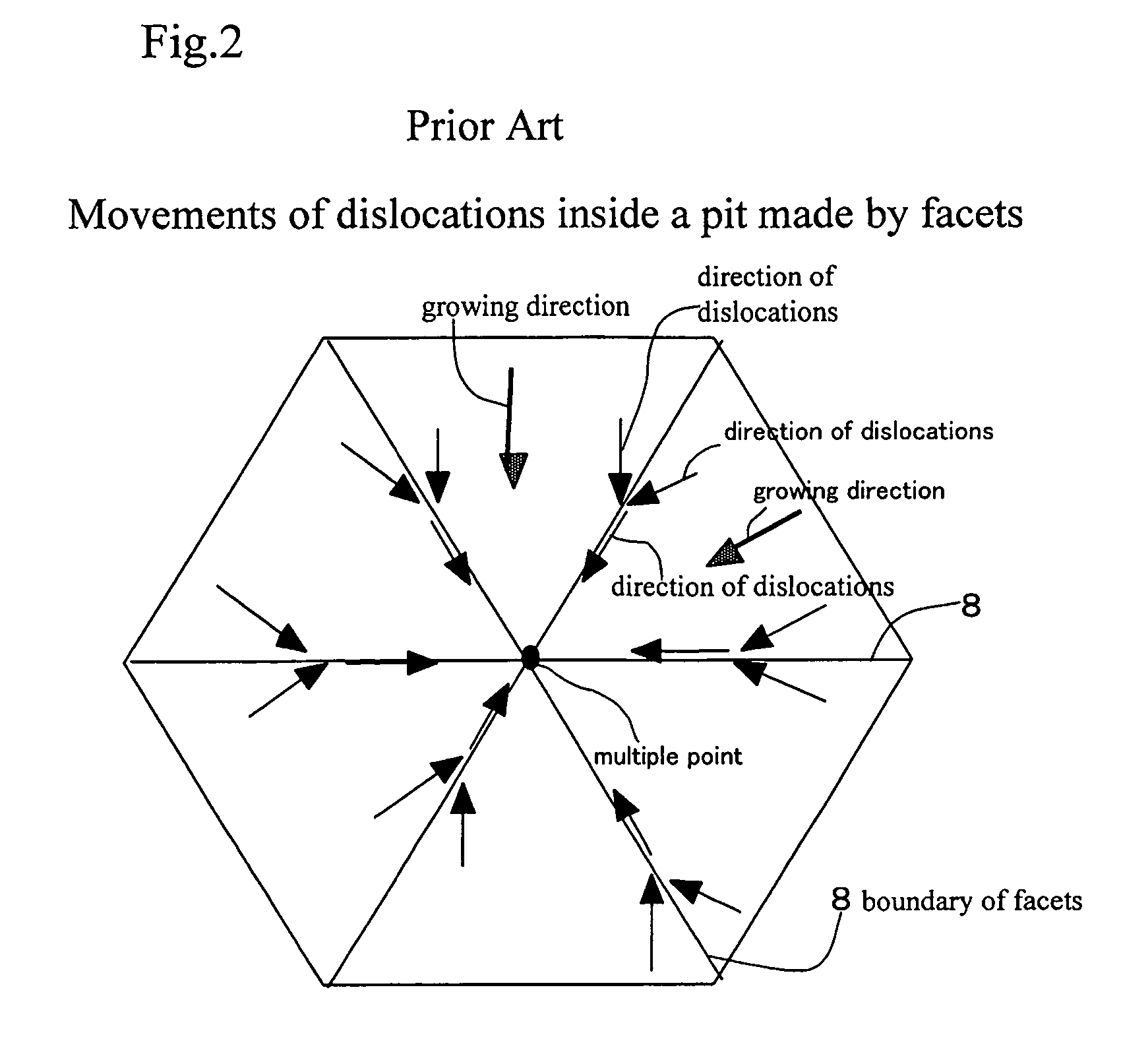
a technology of gan crystal and gan film, which is applied in the direction of crystal growth process, polycrystalline material growth, chemically reactive gases, etc., can solve the problems of difficult separation of sapphire substrates from gan films, inability to make gan single crystals, and inability to eliminate sapphire substrates which are chemically stable and physically rigid

Inactive Publication Date: 2007-12-04
SUMITOMO ELECTRIC IND LTD
View PDF12 Cites 276 Cited by
  • Summary
  • Abstract
  • Description
  • Claims
  • Application Information

AI Technical Summary

Benefits of technology

[0055](2) Edges of the seeds can forcibly resist horizontal invasion of GaN crystal growth and can inhibit GaN crystals from overstepping the seeds for a long time. A thick GaN crystal blanket on a non-seed undersubstrate builds tall conical pit walls which are in contact with the edges of seeds at the bottom. The tall conical pit walls are {11-22} facets in most cases. Conditions (1) and (2) invite a new phenomenon.
[0063]At an early stage, GaN crystals are grown only on non-seeded parts of the undersubstrate. The mask seeds inhibit GaN from growing thereupon. Edges of the seeds strongly prohibit the on-non-seed grown GaN crystal blanket from overrunning thereupon. Round seeds make reverse-conical pits with slanting facets. The slanting facets are also important. The slanting facets, whose feet are sturdily maintained by the seed edges, inhibits GaN crystals from overstepping the seeds. The facets are {11-22} planes in most cases. The inventors noticed that plenty of fine GaN polycrystalline grains are isolatedly dispersed upon the surfaces of the seeds, while the facets can prevent the GaN blanket from overstepping thereon.
[0068]On the contrary, the orientation inversion occurs in the facet-seeded present invention. The present invention assigns orientation-inversion to the crystals overstepping on the seeds by enlarging the protrusions which are inherently orientation-reversed. The existence of fine polycrystalline GaN particles not only prevents GaN crystals from invading on the seed but also plays an important role of reversing orientations on the seeds.
[0075]The pitted GaN blanket 64 and vacant seeds 63 are maintained till an enough thickness. FIG. 5(2) shows a part of the fat GaN blanket 64 and inverse-conical vacant spaces on the mask-seeds 63. High stability of {11-22} and {1-101} facets protects the slanting walls not to landslide.
[0087]As shown in FIG. 5(5), vacant spaces beneath the junction above the seed 63 are filled with GaN granules 72. The filling GaN granules 72 grow downward from the bottom C and F planes of the protrusions. The filling GaN granules take the reverse-orientation since the C and F act as seed crystals. Vacant space above the junction is also filled with GaN granules 65 and 65. The GaN granules 65, which grow on the shallower B and E planes, take the reverse-orientation, since the B and E play a role of a seed. Facet growth of GaN continues without burying the facets. Thus, reverse-oriented GaN grows on the B and E planes. GaN crystals growing on the seed 63 become closed defect accumulating regions (H). GaN crystals growing on the facets 66 become low dislocation single crystal regions (Z), which are otherwise called facet regions. GaN crystals grown on the flat plateau (top) 67 of the GaN blanket become an extra low dislocation single crystal region (Y). The extra low dislocation region (Y) grow with a C-plane on top. Succeeding epitaxial growth sweeps dislocations out of the facet region (Z) and the C-plane region (Y) into the closed defect accumulating region (H). The appearance of the paring protrusions 68 and 68 from the facets 66 confirms the formation of the “reverse-oriented” closed defect accumulating region (H) on the seeds 63. Reverse-oriented single crystalline closed defect accumulating regions (H) are the most reliable, the most endurable, and the most powerful mechanisms for accumulating dislocations. The GaN facet growth proceeds till the blanket attains to a desired thickness.

Problems solved by technology

Czochralski method and Bridgman method which change a melt polycrystal material into a melt, cool a part of the melt and make a large single crystal bulk solid at a thermal equilibrium, are unavailable for making a GaN single crystal.
However, a sapphire substrate which is chemically stable and physically rigid cannot be eliminated after the GaN film has been grown on the sapphire substrate.
However, the separation of the sapphire substrates from the GaN films is difficult even by high power lasers.
However, it is found that thick GaN is not grown upon a GaAs substrate.
Perhaps differences of lattice constants and thermal expansions between GaAs and GaN cause the difficulty of growing thick GaN on the GaAs substrate.
Reduction of dislocations is insufficient.
ELO-made GaN crystals are unsatisfactory as a GaN substrate upon which InGaN type LDs are fabricated.
The inventors noticed that the facet growth method has still problems for producing GaN wafers for making LD chips.
Such high dislocation density 107 cm−2 of the hazy dislocation nebulae is insufficient for making use of the GaN crystal as an LD substrate for making LD devices.
The occurrence of the hazy dislocation nebulae is the first problem of the previous facet growth.
The second problem is planar defect assemblies which are born by gathering dislocations to the pit bottoms and inclining to each other at 60 degrees.
In addition to the hazy dislocation nebulae, the radially extending planar defects assemblies are a serious problem for an LD substrate, since the planar defects would induce degeneration and would restrict lifetime of LDs.
Occurrence and distribution of pits are stochastic, accidental and unprogrammable.
The previous facet growth method which reduces dislocations by growing facet pits without burying, has a weak point of undeterminable positions of pits.
It is impossible to previously determine or know the spots at which facet pits happen.
Uncontrollability of pit positions is a serious problem.
All the three are difficult problems.
The serious problem of the previous facet growth of the inventors which maintains facets and pits without burying the facets was an unstable state of defect assemblies at pit bottoms.
Occurrence of pits and positions of pits were uncontrollable.
However, some problems remain.
Polycrystalline or slanting oriented single crystal closed defect accumulating regions (H) are not the best ones owing to the microcracks caused by the thermal expansion discrepancy between the (H) regions and the other regions.
However, properties and orientations of closed defect accumulating regions (H) depend upon accidents.
It is difficult to always form orientation-inverse, antiparallel single crystal closed defect accumulating regions (H) even on dot-seeded undersubstrates.

Method used


Image

  • Method of growing GaN crystal, method of producing single crystal GaN substrate, and single crystal GaN substrate
  • Method of growing GaN crystal, method of producing single crystal GaN substrate, and single crystal GaN substrate
  • Method of growing GaN crystal, method of producing single crystal GaN substrate, and single crystal GaN substrate

Examples


embodiment 1

1. Growth of GaN Layers on Undersubstrates

[1. Preparation of Undersubstrates]

[0140]A plurality of three kinds of undersubstrate S1, S2, S3 are prepared. All the three kinds of undersubstrate have circular wafers of a 51 mm (2 inches) diameter.[0141]S1. (0001) sapphire (Al2O3) wafer (top surface is a C-plane)[0142]S2. (111) GaAs wafer (top surface is a Ga-surface; A-plane)[0143]S3. (0001) GaN / sapphire wafer (1.5 μm GaN+sapphire) which has been made by coating a 51 mmφ sapphire wafer on which a 1.51 μm-thick GaN film has been grown by an MOCVD method.

[2. Formation of Dotted Seeding Mask]

[0144]Silicon oxide (SiO2) films of a 0.1 μm thickness are deposited by a plasma CVD method on the three kinds of the undersubstrates. The mask consists of dotted round seeds regularly populated on the undersubstrate.

[0145]The mask seeds are made by photolithography, which has steps of coating the SiO2 / undersubstrates with a resist, exposing the resist via four different stripe patterned photomasks, et...

embodiment

Preferred Embodiment

[0229]Round Wafer[0230]Diameter; 50 mmφ,[0231]Thickness; 400 μm

[0232]Rectangular wafers have an advantage of facilitating the identification of resonator mirror planes in fabricating laser diodes. One of the sides of the rectangular wafers coincides with the resonator mirror planes.

[0233]Circular wafers, which have rotation symmetry, exhibit an advantage of enabling material gases to make uniform streams and to synthesize uniform epitaxial films without epitaxy anomalies. Smaller wafers having a size less than 10 mm induce random gas flows and incur epitaxy anomalies at wafer edges. Large wafers bigger than a 160 mm diameter invite large distortion heights. The present invention takes, for example, gallium arsenide (GaAs) wafers as undersubstrates. The maximum size of the GaAs wafer sold on the market is 150 mmφ (six inches) at present.

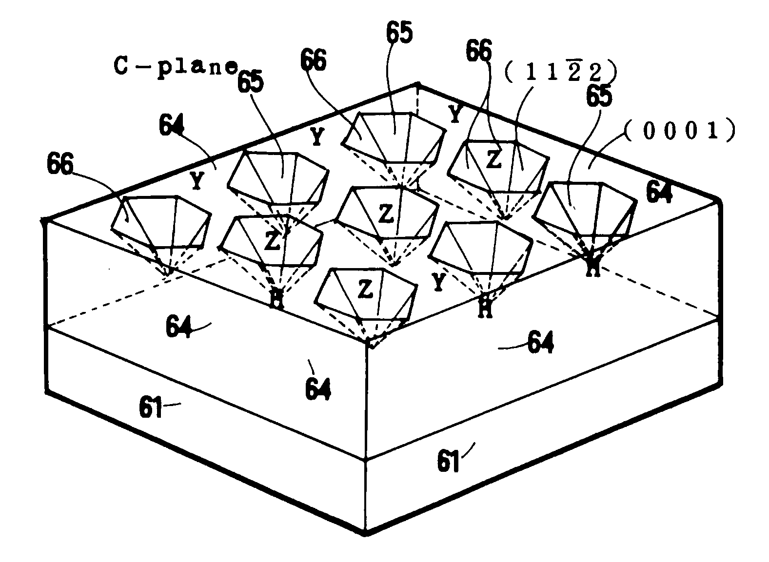
(9) Three Dimensional Structure (FIG. 8)

[0234]Widths of the H, Y and Z regions vary in the progress of crystal growth. H and Y di...

example 1 (

TEM OBSERVATION)

[0237]A GaN wafer made by the method of the present invention shows dislocation distribution on H, Z and Y as follows.[0238]H; 1×107 cm−2-2×107 cm−2 [0239]Z; 1×105 cm−2-1×107 cm−2 [0240]Y; 2×104 cm−2-2×105 cm−2


PUM

PropertyMeasurementUnit
temperatureaaaaaaaaaa

Abstract

Dotted seeds are implanted in a regular pattern upon an undersubstrate. A GaN crystal is grown on the seed implanted undersubstrate by a facet growth method. The facet growth makes facet pits above the seeds. The facets assemble dislocations from neighboring regions, accumulate the dislocations into pit bottoms, and make closed defect accumulating regions (H) on the seeds. The polycrystalline or slanting orientation single crystal closed defect accumulating regions (H) induce microcracks due to thermal expansion anisotropy. The best one is orientation-inversion single crystal closed defect accumulating regions (H). At an early stage, orientation-inverse protrusions are induced on tall facets and unified with each other above the seeds. Orientation-inverse crystals growing on the unified protrusions become the orientation-inverse single crystal closed defect accumulating regions (H).

Description

CROSS REFERENCE TO RELATED APPLICATIONS[0001]This application is a continuation-in-part of and claims priority to U.S. patent application Ser. No. 10 / 700,495, filed on Nov. 5, 2003, now U.S. Pat. No. 7,112,826 entitled “SINGLE CRYSTAL GaN SUBSTRATE, METHOD OF GROWING SAME AND METHOD OF PRODUCING SAME” by Kensaku MOTOKI et al.BACKGROUND OF THE INVENTION[0002]1. Field of the Invention[0003]This invention relates to a single crystal gallium nitride (GaN) substrate for producing blue light emitting diodes (LEDs) and blue light laser diodes (LDs) composed of group 3-5 nitride type semiconductors, to a method of producing a single crystal gallium nitride substrate, and to a method of growing a GaN crystal.[0004]Blue light emitting diodes (LEDs) based upon the group 3-5 nitride type semiconductors (InGaN, GaN) have been manufactured, sold and used on a large scale. Almost all the practical nitride type LEDs are made upon insulating sapphire (α-Al2O3) substrates. Sapphire belongs to trigona...

Claims


Application Information

Patent Timeline
Patent Type & Authority Patents(United States)
IPC IPC(8): C30B25/00C30B25/18C30B29/40
CPCC30B29/40C30B25/18
Inventor MOTOKI, KENSAKUOKAHISA, TAKUJIHIROTA, RYUNAKAHATA, SEIJIUEMATSU, KOJI
Owner SUMITOMO ELECTRIC IND LTD
Why Eureka
Try Eureka